News Posts matching #Sunny Cove

Return to Keyword Browsing

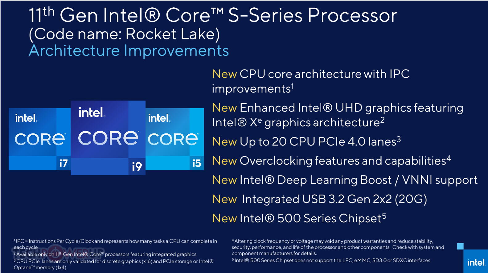
Latency Increase from Larger L2 Cache on Intel "Raptor Cove" P-core Well Contained: Report

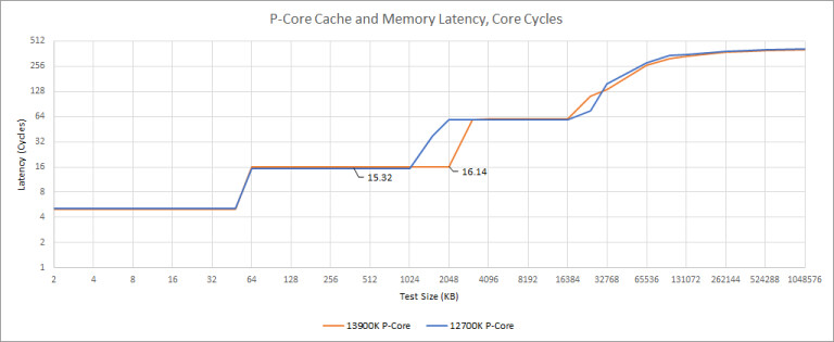
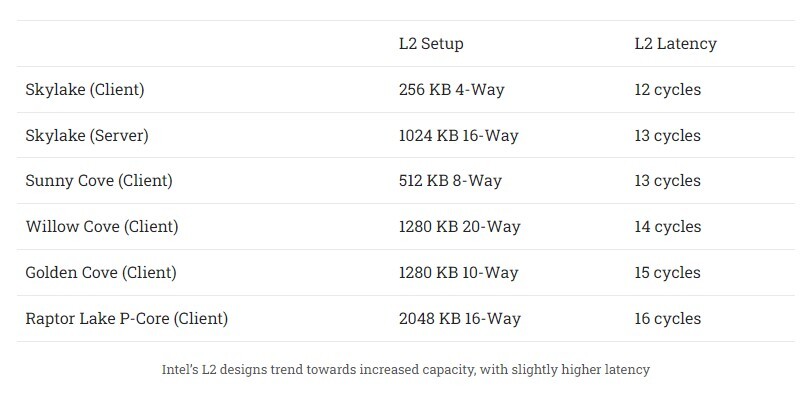
According to an investigative report by "Chips and Cheese," the larger L2 caches in Intel's 13th Gen Core "Raptor Lake-S" doesn't come with a proportionate increase in cache latency, and Intel seems to have contained the latency increase well. "Raptor Lake-S" significantly increases L2 cache sizes over the previous generation. Each of its 8 "Raptor Cove" P-cores has 2 MB of dedicated L2 cache, compared to the 1.25 MB with the "Golden Cove" P-cores powering the current-gen "Alder Lake-S," which amounts to a 60 percent increase in size. The "Gracemont" E-core clusters (group of four E-cores), sees a doubling in the size of the L2 cache that's shared among the four cores in the cluster, from 2 MB in "Alder Lake," to 4 MB. The last-level L3 cache shared among all P-cores and E-core clusters, sees a less remarkable increase in size, from 30 MB to 36 MB.

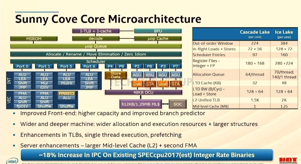
Larger caches have a direct impact on performance, as more data is available close to the CPU cores, sparing them a lengthy fetch/store operation to the main memory (RAM). However, making caches larger doesn't just cost die-area, transistor-count, and power/heat, but also latency, even though L2 cache is an order of magnitude faster than the L3 cache, which in turn is significantly faster than DRAM. Chips and Cheese tracked and tabulated the L2 cache latencies of past Intel client microarchitectures, and found a generational increase in latencies with increasing L2 cache sizes, leading up to "Alder Lake." This increase has somehow tapered with "Raptor Lake."

Intel Launches Xeon D Processor Built for the Network and Edge

Today, ahead of MWC Barcelona 2022, Intel launched new Intel Xeon D processors: the D-2700 and the D-1700. They are Intel's newest system-on-chip (SoC) built for the software-defined network and edge, with integrated AI and crypto acceleration, built-in Ethernet, support for Intel Time Coordinated Computing (Intel TCC) and Time Sensitive Networking (TSN), and industrial-class reliability. New Intel Xeon D processors extend compute with acceleration beyond the core data center, generating a better overall experience for key network and edge usages and workloads.

"As the industry enters a world of software-defined everything, Intel is delivering programmable platforms for networking and the edge to enable one of the most significant transformations our industry has ever seen. The new Intel Xeon D processor is built for this. Based on the proven and trusted Intel architecture, this processor is designed for a range of use cases to unleash innovation across the network and edge," said Dan Rodriguez, Intel corporate vice president, Network & Edge Group, general manager of the Network Platforms Group.

Intel's Upcoming Sapphire Rapids Server Processors to Feature up to 56 Cores with HBM Memory

Intel has just launched its Ice Lake-SP lineup of Xeon Scalable processors, featuring the new Sunny Cove CPU core design. Built on the 10 nm node, these processors represent Intel's first 10 nm shipping product designed for enterprise. However, there is another 10 nm product going to be released for enterprise users. Intel is already preparing the Sapphire Rapids generation of Xeon processors and today we get to see more details about it. Thanks to the anonymous tip that VideoCardz received, we have a bit more details like core count, memory configurations, and connectivity options. And Sapphire Rapids is shaping up to be a very competitive platform. Do note that the slide is a bit older, however, it contains useful information.

The lineup will top at 56 cores with 112 threads, where this processor will carry a TDP of 350 Watts, notably higher than its predecessors. Perhaps one of the most interesting notes from the slide is the department of memory. The new platform will make a debut of DDR5 standard and bring higher capacities with higher speeds. Along with the new protocol, the chiplet design of Sapphire Rapids will bring HBM2E memory to CPUs, with up to 64 GBs of it per socket/processor. The PCIe 5.0 standard will also be present with 80 lanes, accompanying four Intel UPI 2.0 links. Intel is also supposed to extend the x86_64 configuration here with AMX/TMUL extensions for better INT8 and BFloat16 processing.

Intel 3rd Gen Xeon Scalable Launch Event Liveblog

Intel today is launching its 3rd Generation Xeon Scalable processor bringing its first major IPC uplift to the enterprise space in five years. The Xeon Scalable processors are built on the 10 nm SuperFin process, and the "Ice Lake-SP" microarchitecture that bring new "Sunny Cove" CPU cores to the server space, including support for PCI-Express 4.0 I/O capabilities, a wider memory interface, and a more feature-rich AVX-512 instruction-set, along with DLBoost for HPC. join us for its launch live-blog.

14:59 UTC: CEO Pat Gelsinger and Data Platforms group head Navin Shenoy are expected to take centerstage. Xeon and memory group head Lisa Spelman could announce relevant platform products. This is Gelsinger's first major launch since taking office.

15:01 UTC: What will you solve for?

Intel Starts Production of "Ice Lake" Xeons, Ships 11th Gen Core "Rocket Lake-S"

Intel in its FY 2020 + Q4 2020 earnings release revealed two important development milestones from its two core businesses. As part of its Q4 2020 business highlights disclosures, the company revealed that it has commenced mass-production of its next-generation Xeon Scalable "Ice Lake-SP" enterprise processors. These chips implement the "Ice Lake" microarchitecture, with "Sunny Cove" CPU cores that offer higher IPC over "Cascade Lake," and are built on the company's 10 nm silicon fabrication node. Our older article details the 10 nm "Ice Lake-SP" silicon, where each die offers up to 28 cores, and enables Intel to build processors with up to 56 cores using two such dies on multi-chip modules.

Next up, the company states that it has "started shipping" its 11th Gen Core "Rocket Lake-S" desktop processors. "Shipping" in this context could even mean commencement of mass-production, and transfer of inventory down the supply chain, in the build up to a market availability date. At its digital keynote address on the sidelines of the 2021 International CES, Intel revealed many more details of "Rocket Lake-S," including its flagship Core i9-11900K 8-core processor, which it claims retakes the gaming performance lead that the company recently lost to AMD's Ryzen 5000 series. Multiple sources confirmed that these processors should be available only after mid-March, 2021.

Intel Confirms Rocket Lake-S Features Cypress Cove with Double-Digit IPC Increase

Today, Intel has decided to surprise us and give an update to its upcoming CPU lineup for desktop. With the 11th generation, Core CPUs codenamed Rocket Lake-S, Intel is preparing to launch the new lineup in the first quarter of 2021. This means that we are just a few months away from this launch. When it comes to the architecture of these new processors, they are going to be based on a special Cypress Cove design. Gone are the days of Skylake-based designs that were present from the 6th to 10th generation processors. The Cypress Cove, as Intel calls it, is an Ice Lake adaptation. Contrary to the previous rumors, it is not an adaptation of Tiger Lake Willow Cove, but rather Ice Lake Sunny Cove.

The CPU instruction per cycle (IPC) is said to grow in double-digits, meaning that the desktop users are finally going to see an improvement that is not only frequency-based. While we do not know the numbers yet, we can expect them to be better than the current 10th gen parts. For the first time on the Intel platform for desktops, we will see the adoption of PCIe 4.0 chipset, which will allow for much faster SSD speeds and support the latest GPUs, specifically, there will be 20 PCIe 4.0 lanes coming from the CPU only. The CPU will be paired with 12th generation Xe graphics, like the one found in Tiger Lake CPUs. Other technologies such as Deep Learning Boost and VNNI, Quick Sync Video, and better overclocking tuning will be present as well. Interesting thing to note here is that the 10C/20T Core i9-10900K has a PL1 headroom of 125 W, and 250 W in PL2. However, the 8C/16T Rocket Lake-S CPU also features 125 W headroom in PL1, and 250 W in PL2. This indicates that the new Cypress Cove design runs hotter than the previous generation.

Intel Xeon Scalable "Ice Lake-SP" 28-core Die Detailed at Hot Chips - 18% IPC Increase

Intel in the opening presentation of the Hot Chips 32 virtual conference detailed its next-generation Xeon Scalable "Ice Lake-SP" enterprise processor. Built on the company's 10 nm silicon fabrication process, "Ice Lake-SP" sees the first non-client and non-mobile deployment of the company's new "Sunny Cove" CPU core that introduces higher IPC than the "Skylake" core that's been powering Intel microarchitectures since 2015. While the "Sunny Cove" core itself is largely unchanged from its implementation in 10th Gen Core "Ice Lake-U" mobile processors, it conforms to the cache hierarchy and tile silicon topology of Intel's enterprise chips.

The "Ice Lake-SP" die Intel talked about in its Hot Chips 32 presentation had 28 cores. The "Sunny Cove" CPU core is configured with the same 48 KB L1D cache as its client-segment implementation, but a much larger 1280 KB (1.25 MB) dedicated L2 cache. The core also receives a second fused multiply/add (FMA-512) unit, which the client-segment implementation lacks. It also receives a handful new instruction sets exclusive to the enterprise segment, including AVX-512 VPMADD52, Vector-AES, Vector Carry-less Multiply, GFNI, SHA-NI, Vector POPCNT, Bit Shuffle, and Vector BMI. In one of the slides, Intel also detailed the performance uplifts from the new instructions compared to "Cascade Lake-SP".

Intel "Willow Cove" Core, Xe LP iGPU, and "Tiger Lake" SoC Detailed

A lot is riding for Intel on its 11th Gen Core "Tiger Lake" system-on-chip (SoC), which will launch exclusively on mobile platforms, hoping to dominate the 7 W thru 15 W ultraportable form-factors in 2020, while eventually scaling up to the 25 W thru 45 W H-segment form-factors in 2021, with a variant that is rumored to double core-counts. The chip is built on Intel's new 10 nm SuperFin silicon fabrication node that enables a double digit percentage energy efficiency growth over 10 nm, allowing Intel to significantly dial up clock speeds without impacting the power envelope. The CPU and iGPU make up the two key components of the "Tiger Lake" SoC.

The CPU component on the "Tiger Lake" processors that launch in a few weeks from now features four "Willow Cove" CPU cores. Coupled with HyperThreading, this ends up being a 4-core/8-thread setup, although much of Intel's innovation is in giving these cores significant IPC increases over the "Skylake" core powering "Comet Lake" processors, and compared to the "Sunny Cove" cores powering "Ice Lake" a minor IPC (although major net performance increase from clock speeds). The "Willow Cove" CPU core appears to be a derivative of the "Sunny Cove" core, designed to take advantage of the 10 nm SuperFin node, along with three key innovations.

NUVIA Phoenix SoC is 40-50 Percent Faster Than Zen 2 for a Third of Power

Last year, in November of 2019, a startup company called NUVIA Inc. broke out of the stealth mode and decided to reveal itself to the public. Focused on "re-imagining silicon", the company is led by some of the brightest minds in the semiconductor industry. Some people like Gerard Williams III, the CEO of the company, previously served as a chief CPU architect at Apple and has spent over 10 years at Arm before that. Others like Manu Gulati and John Bruno serve as senior vice presidents of silicon and system engineering respectively. Together, their people are forming a company full of well-known industry names. Of course, there are more and you should check out this page.

NUVIA Inc. promises to deliver only the best performance and "re-imagine silicon" as they say. Today, we got some bold claims from the company regarding the performance of their upcoming Phoenix SoC. Using Geekbench 5, the company has provided some simulated results of how the Phoenix SoC will perform. Being that it runs on Arm ISA, the SoC can run at very low power and achieve good performance. NUVIA has run some simulations and it expects its Phoenix SoC to be 40-50% faster in single-threaded performance than Zen 2/Sunny Cove at just a third of the power, 33% of the percent of power to be precise. In the graph below, NUVIA has placed its SoC only in 5 W range, however, the company said that they have left the upper curve to be disclosed at later date, meaning that the SoC will likely compete in high-performance markets and at higher power targets. While these claims are to be taken with a grain of salt, it is now a waiting game to see how NUVIA realizes its plans.
NUVIA Inc. Logo NUVIA Phoenix SoC Performance

Intel Linux Patch Confirms "Alder Lake" is a Hybrid Core Processor

A Linux kernel patch contributed and signed off by Intel confirms that its upcoming Core "Alder Lake" processor will feature a hybrid core topology, much like Core Hybrid "Lakefield." The patch references "Lakefield" and "Alder Lake" under "Hybrid Core/Atom Processors." The patch possibly gives the Linux kernel awareness of the hybrid core topology, so it can schedule its work between the two types of cores on the silicon accordingly, and avoid rotating between the two core groups. Under the Android project, Linux has been aware of a similar tech from Arm since 2013.

Analogous with Arm big.LITTLE, the Intel Hybrid Core technology involves two kinds of CPU cores on a processor die, the first kind being "high performance," and the second being "low power." On "Lakefield," Intel deployed one "Sunny Cove" high performance core, and four "Tremont" low power cores. The low power cores keep the machine ticking through the vast majority of time when processing workloads requiring the high performance cores aren't present. With "Alder Lake," Intel is expected to scale up this concept, with the silicon rumored to feature eight "Golden Cove" high performance cores, and eight "Gracemont" low power ones. The chip is also expected to feature a Gen12 Xe iGPU.

Windows 10 Scheduler Aware of "Lakefield" Hybrid Topologies, Benchmarked

A performance review of the Intel Core i5-L16G7 "Lakefield" Hybrid processor (powering a Samsung Galaxy S notebook) was recently published by Golem.de, which provides an in-depth look at Intel's ambitious new processor design that sets in motion the two new philosophies Intel will build its future processors on - packaging modularity provided by innovative new chip packaging technologies such as Foveros; and Hybrid processing, where there are two sets of CPU cores with vastly different microarchitectures and significantly different performance/Watt curves that let the processor respond to different kinds of workloads while keeping power-draw low. This concept was commercially proliferated first by Arm, with its big.LITTLE topology that took to the market around 2013. The "Lakefield" i5-L16G7 combines a high-performance "Sunny Cove" CPU core with four smaller "Tremont" cores, and Gen11 iGPU.

The Golem.de report reveals that Windows 10 thread scheduler is aware of the hybrid multi-core topology of "Lakefield," and that it is able to classify workloads at a very advanced level so the right kind of core is in use at any given time. The "Sunny Cove" core is called upon when interactive vast serial processing loads are in demand. This could even be something like launching applications, new tabs in a multi-process web-browser, or less-parallelized media encoding. The four "Tremont" cores keep the machine "cruising," handling much of the operational workload of an application, and is also better tuned to cope with highly parallelized workloads. This is similar to a hybrid automobile, where the combustion engine provides tractive effort from 0 kph, while the electric motor sustains a cruising speed.

Intel Lakefield Core i5-L16G7 Performance Benchmarks Leak

Performance benchmarks have started leaking for Intel-s upcoming Lakefield CPUs - low-power SoCs designed with Intel's latest technology. The Lakefield family of CPUs will make use of an Arm-similar big.LITTLE design, where this particular CPU, the Core i5-L16G7, will ship with four low-power "Tremond" cores and one large, high-performance "Sunny Cove" core for peak workloads. Built using Intel's Foveros stacking technology, these are the first chips to be built on Intel's modular platform, which should allow for pairing of I/O dies, chiplet-like CPU arrangements and memory in a 3D package. Physical distance reductions impact latency and power consumption, which should allow for an interesting design result.

Notebookcheck has tested an Intel Lakefield Core i5-L16G7 CPU that's being deployed on upcoming Samsung's Galaxy Book S, and the results are sort of a mixed bag. For one, Intel's Lakefield seems to be around 67% slower than the company's previous ultra-low-power architecture, Amber Lake. Something of this might have been caused by the fact that the Lakefield CPU didn't boost towards its advertised 3.0 GHz; it only managed to reach 2.4 GHz, which obviously hampered performance. Perhaps pre-release silicon is the culprit, or perhaps it's the galaxy Book S that's been configured with more restrictive thermal and power characteristics than the chip was actually designed to run at. The chip did manage to run the FireStrike test beating the Amber Lake-based Acer Swift 7 by 23%, though, so not all is looking bleak.

Possible Intel "Ice Lake-SP" 24-core Xeon Processor Surfaces on Geekbench Database

Intel plans to update its Xeon Scalable server processor family this year with the new "Ice Lake-SP" microarchitecture. Built on the 10 nm+ silicon fabrication process, "Ice Lake-SP" is a high- thru extreme core-count monolithic silicon that features "Sunny Cove" CPU cores that introduce the first real IPC increases over "Skylake." A 24-core/48-thread processor likely based on this silicon surfaced on the Geekbench database, where it posted some impressive numbers given its low clock speeds.

The processor comes with an identification string "GenuineIntel Family 6 Model 106 Stepping 4," with a nominal clock speed of 2.20 GHz, and boost frequency of 2.90 GHz, which points to the possibility of this being an engineering sample. Besides clock speeds and core counts, some basic hardware specs were detected by Geekbench 4. For starters, the processor has an L1D cache size of 48 KB and L1I cache size of 32 KB, which is similar to the client-segment "Ice Lake-U" silicon based Core i7-1065G7, and confirms that this processor uses "Sunny Cove" cores. "Cascade Lake" and "Skylake" cores use 32 KB L1D caches. Also, the dedicated L2 cache per core is 1.25 MB, up from the 1 MB L2 caches on "Cascade Lake." Client-segment "Ice Lake" chips use 512 KB L2 caches. The shared L3 cache is 36 MB (or 1.5 MB slice per core), which loosely aligns with the cache balance of Intel's server and HEDT processors. In this bench run, the processor is backed by 256 GB of memory, of an unknown type or configuration. In the three bench runs, the setup scores roughly 4100 points single-core, and roughly 42000 points multi-core.

First Intel "Lakefield" Powered Samsung Galaxy Book S Listed on the Company's Canadian Store

One of the first Intel "Lakefield" heterogenous processor-powered devices, a Samsung Galaxy Book S model, is listed by Samsung on its Canadian online store. The Galaxy Book series typically consists of Arm-powered clamshell/convertible notebooks that use Windows 10 (Arm version). The device in question is a Galaxy Book S 13.3-inch notebook bearing model number NP767XCM-K01CA, and comes in two color trims - "Mercury Gray" and "Earthy Gold."

Under the hood is an Intel Core i5-L16G7 "Lakefield" heterogenous processor that has four "Tremont" low-power cores, and a "Sunny Cove" high-performance cores, in an arrangement rivaling Arm big.LITTLE, the first of many such chips from the company, as it taps into new technologies such as heterogenous cores and advanced Foveros chip packaging to design its future processors. The notebook offers Full HD resolution, 8 GB of RAM, 256 GB or 512 GB of solid-state NVMe storage, 802.11ax 2x2 WLAN, and a 42 Wh battery, possibly with double-digit hour battery life. All of this goes into a 6.2 mm (folded) device weighing under a kilogram.

Intel "Tiger Lake" and "Lakefield" to Launch Around September-October, 2020

The 11th generation Intel Core "Tiger Lake" mobile processor and pioneering "Lakefield" heterogenous x86 processor could debut around September or October, 2020, according to a leaked Lenovo internal slide posted by NotebookCheck. It also points to Intel denoting future processors' lithography with Foveros 3D Packaging as simply "3D," and not get into a nanometer number-game with AMD (which is now in 7 nm and on course to 5 nm in 2022). This makes sense as Foveros allows the combination of dies built on different silicon fabrication nodes.

"Tiger Lake" is still denoted as a 10 nm as it's a planar chip. Intel is developing it on a refined 10 nm+ silicon fabrication process, which apparently enables Intel to increase clock speeds without breaking the target power envelope. "Tiger Lake" sees the commercial debut of Intel's ambitious Xe graphics architecture as an iGPU solution. "Lakefield," on the other hand, is a 5-core processor combining four "Tremont" low power x86-64 cores with a "Sunny Cove" high-powered core, in a setup rivaling Arm big.LITTLE, enabling the next generation of mobile computing form-factors, which Intel and its partners are still figuring out under Project Athena.

Intel 10nm Product Lineup for 2020 Revealed: Alder Lake and Ice Lake Xeons

A leaked Intel internal slide surfaced on Chinese social networks, revealing five new products the company will build on its 10 nm silicon fabrication process. These include the "Alder Lake" heterogenous desktop processor, "Tiger Lake" mobile processor, "Ice Lake" based Xeon Scalable enterprise processors, DG1 discrete GPU, and "Snow Ridge" 5G base-station SoC. Some, if not all of these products, will implement Intel's new 10 nm+ silicon fabrication node that is expected to go live within 2020.

"Alder Lake" is a desktop processor that implements Intel's new heterogenous x86 core design that's making its debut with "Lakefield." The chip features up to 8 larger "Willow Cove" or "Golden Cove" CPU cores, and up to 8 smaller "Tremont" or "Gracemont" cores. This 8-big/8-small combo lets the chip achieve TDP targets around 80 Watts. Next up is "Tiger Lake," Intel's next-generation mobile processor family succeeding "Ice Lake." This microarchitecture implements "Willow Cove" CPU cores in a homogeneous setup, alongside Xe architecture based integrated graphics. "Ice Lake-SP" is Intel's next enterprise architecture that places mature "Sunny Cove" CPU cores in extreme core-count dies. Lastly, there's "Snow Ridge," an SoC purpose built for 5G base-stations. Image quality notwithstanding, these slides don't appear particularly new, and it's likely that COVID-19 has destabilized the roadmap. For instance, "Alder Lake," and "Ice Lake-SP" are expected to be 10 nm++ chips, a node that doesn't go live before 2021.

Trio of Intel 10th Gen "Ice Lake" NG Processors Show Up on Intel Website

Three new 10th generation Core "Ice Lake-U" notebook processors surfaced on Intel website with a curious new nomenclature, possibly ahead of their "Q2-2020" launch. The three follow the processor model numbering convention of 10x0NGy, where x denotes the key model differentiator, and y the iGPU tier differentiator. Among the three parts are the Core i7-1060NG7, the Core i5-1030NG7, and the Core i3-1000NG4. The i5-1060NG7 and i5-1030NG7 are 10-Watt parts and feature 4-core/8-thread "Sunny Cove" CPUs, while the i3-1000NG4 packs a 2-core/4-thread "Sunny Cove" CPU, and is rated at 9 W TDP.

What sets the Core i5 apart from the Core i7, besides CPU clock speeds, are L3 cache sizes: 8 MB for the Core i7, and 6 MB for the i5. The Core i3 packs 4 MB. With an eye clearly on ultra-portable notebooks, these chips only feature dual-channel LPDDR4 memory interfaces, with memory clock speeds of up to 3733 MT/s. The i7-1060NG7 CPU ticks at 1.20 GHz and up to 3.80 GHz Turbo Boost; while the i5-1030NG7 runs between 1.10 GHz to 3.50 GHz. The i3-1000NG4 is clocked 1.10 GHz with 3.20 GHz Turbo Boost. The Core i7 and Core i5 parts pack an identical Gen11 iGPU: Iris Plus clocked between 300 MHz to 1.10 GHz for the i7 and up to 1.05 GHz for the i5. The Core i3 features 300-900 MHz iGPU clock speeds and fewer execution units.

Intel Core i5-L15G7 Lakefield Processor Spotted

Intel has been experimenting with a concept of mixing various types of cores in a single package with a design called Lakefield. With this processor, you would get a package of relatively small dimensions that are 12-by-12-by-1 millimeters withing very low TDP. Thanks to the Twitter user InstLatX64 (@InstLatX64) we have some GeekBench 5 results of the new Lakefield chip. The CPU in question is the Core i5-L15G7, a 5 core CPU without HyperThreading. The 5C/5T would be a weird configuration if only Lakefield wasn't meant for such configs. There are one "big" Sunny Cove core and four "small" Tremont cores built on the 10 nm manufacturing process. This is the so-called compute die, where only the CPU cores are present. The base dies containing other stuff like I/O controllers and PHYs, memory etc. is made on a low-cost node like 22 nm, where performance isn't the primary target. The whole chip is targeting the 5-7 W TDP range.

In the GeekBench 5 result we got, the Core i5-L15G7 is a processor that has a base frequency of 1.4 GHz, while in the test it reached as high as 2.95 GHz speeds. This is presumably for the big Sunny Cove cores, as Tremont cores are supposed to be slower. The cache configuration reportedly puts 1.5 MB of L2$ and 4 MB of L3$ for the CPUs. If we take a look at performance numbers, the chip scores 725 points in single-core tests, while the multi-core result is 1566 points. We don't know what is the targeted market and what it competes with, however, if compared to some offerings from Snapdragon, like the Snapdragon 835, it offers double the single-threaded performance with a similar multi-core score. If this is meant to compete with the more powerful Snapdragon offerings like the 8cx model, comparing the two results in Intel's fail. While the two have similar single-core performance, the Snapdragon 8cx leads by as much as 76.9% in a multi-core scenario, giving this chip a heavy blow.
Intel Core i5-L15G7 Intel Lakefield

Intel Zooms in on "Lakefield" Foveros Package

The fingernail-size Intel chip with Foveros technology is a first-of-its kind. With Foveros, processors are built in a totally new way: not with the various IPs spread out flat in two dimensions, but with them stacked in three dimensions. Think of a chip designed as a layer cake (a 1-millimeter-thick layer cake) versus a chip with a more-traditional pancake-like design. Intel's Foveros advanced packaging technology allows Intel to "mix and match" technology IP blocks with various memory and I/O elements - all in a small physical package for significantly reduced board size. The first product designed this way is "Lakefield," the Intel Core processor with Intel hybrid technology.

Industry analyst firm The Linley Group recently named Intel's Foveros 3D-stacking technology as "Best Technology" in its 2019 Analysts' Choice Awards. "Our awards program not only recognizes excellence in chip design and innovation, but also acknowledges the products that our analysts believe will have an impact on future designs," said Linley Gwennap, of The Linley Group.

Intel Core i5-L16G7 is the first "Lakefield" SKU Appearance, Possible Prelude to New Nomenclature?

Intel Core i5-L16G7 is the first commercial SKU that implements Intel's "Lakefield" heterogenous x86 processor architecture. This 5-core chip features one high-performance "Sunny Cove" CPU core, and four smaller "Tremont" low-power cores, with an intelligent scheduler balancing workloads between the two core types. This is essentially similar to ARM big.LITTLE. The idea being that the device idles most of the time, when lower-powered CPU cores can hold the fort; performance cores kick in only when really needed, until which time they remain power-gated. Thai PC enthusiast TUM_APISAK discovered the first public appearance of the i5-L16G7 in an unreleased Samsung device that has the Userbenchmark device ID string "SAMSUNG_NP_767XCL."

Clock speeds of the processor are listed as "1.40 GHz base, with 1.75 GHz turbo," but it's possible that the two core types have different clock-speed bands, just like the cores on big.LITTLE SoCs. Other key components of "Lakefield" include an iGPU based on the Gen11 graphics architecture, and an LPDDR4X memory controller. "Lakefield" implements Foveros packaging, in which high-density component dies based on newer silicon fabrication nodes are integrated with silicon interposers based on older fabrication processes, which facilitate microscopic high-density wiring between the dies. In case of "Lakefield," the Foveros package features a 10 nm "compute field" die sitting atop a 22 nm "base field" interposer.

Intel Unveils Xe DG1-SDV Graphics Card, Demonstrates Intent to Seriously Compete in the Gaming Space

At a media event on Wednesday, Intel invited us to check out their first working modern discrete graphics card, the Xe DG1 Software Development Vehicle (developer-edition). Leading the event was our host Ari Rauch, Intel Vice President and General Manager for Graphics Technology Engineering and dGPU Business. Much like gruff developer-editions of game consoles released to developers several quarters ahead of market launch, the DG1-SDV allows software developers to discover and learn the Xe graphics architecture, and develop optimization processes for their current and future software within their organizations. We walked into the event expecting to see a big ugly PCB with a bare fan-heatsink and a contraption that sort-of looks like a graphics card; but were pleasantly surprised with what we saw: a rather professional product design.

What we didn't get at the event, through, was a juicy technical breakdown of the Xe graphics architecture, and its various components that add up to the GPU. We still left pleasantly surprised for what we were shown: it works! The DG1-SDV is able to play games at 1080p, even if they are technically lightweight titles like "Warframe," and aren't maxing out settings. The SDV is a 15.2 cm-long graphics card that relies on the PCI-Express slot for power entirely (and hence pulling less than 75 W).

Intel "Rocket Lake" an Adaptation of "Willow Cove" CPU Cores on 14nm?

The "Willow Cove" CPU core design succeeds "Sunny Cove," Intel's first truly new CPU core design in close to 5 years. "Sunny Cove" is implemented in the 10 nm "Ice Lake" microarchitecture, and "Willow Cove" cores are expected to debut with the 10 nm+ "Tiger Lake." It turns out that Intel is working to adapt "Willow Cove" CPU cores onto a 14 nm microarchitecture, and "Rocket Lake" could be it.

Twitter user @chiakokhua, a retired VLSI engineer with high hit-rate on CPU microarchitecture news, made sense of technical documents to point out that "Rocket Lake" is essentially a 14 nm adaptation of "Tiger Lake," but with the iGPU shrunk significantly, to make room for the larger CPU cores. The Gen12 iGPU on "Rocket Lake-S" will feature just 32 execution units (EUs), whilst on "Tiger Lake," it has three times the muscle, with 96 EUs. "Rocket Lake" also replaces "Tiger Lake's" FIVR (fully-integrated voltage regulation) with a conventional SVID VRM architecture.

Microsoft Unveils First Intel "Lakefield" Device and Surface Lineup with 10th Gen Core

Today, at a launch event in New York City, Microsoft previewed the Surface Neo, a category-defining device co-engineered with Intel. The dual-screen device will be powered by Intel's unique processor, code-named "Lakefield," that features an industry-first architecture combining a hybrid CPU with Intel's Foveros 3D packaging technology. It offers device-makers more flexibility to innovate on design, form factor and experience.

"The innovation we've achieved with Lakefield gives our industry partners the ability to deliver on new experiences, and Microsoft's Neo is trailblazing a new category of devices. Intel is committed to pushing the boundaries of computing by delivering key technology innovations for partners across the ecosystem," said Gregory Bryant, Intel executive vice president and general manager of the Client Computing Group.

Intel "Ice Lake" IPC Best-Case a Massive 40% Uplift Over "Skylake," 18% on Average

Intel late-May made its first major disclosure of the per-core CPU performance gains achieved with its "Ice Lake" processor that packs "Sunny Cove" CPU cores. Averaged across a spectrum of benchmarks, Intel claims a best-case scenario IPC (instructions per clock) uplift of a massive 40 percent over "Skylake," and a mean uplift of 18 percent. The worst-case scenario sees its performance negligibly below that of "Skylake." Intel's IPC figures are derived entirely across synthetic benchmarks, which include SPEC 2016, SPEC 2017, SYSMark 2014 SE, WebXprt, and CineBench R15. The comparison to "Skylake" is relevant because Intel has been using essentially the same CPU core in the succeeding three generations that include "Kaby Lake" and "Coffee Lake."

A Chinese tech-forum member with access to an "Ice Lake" 6-core/12-thread sample put the chip through the CPU-Z internal benchmark (test module version 17.01). At a clock-speed of 3.60 GHz, the "Ice Lake" chip allegedly achieved a single-core score of 635 points. To put this number into perspective, a Ryzen 7 3800X "Matisse" supposedly needs to run at 4.70 GHz to match this score, and a Core i7-7700K "Kaby Lake" needs to run at 5.20 GHz. Desktop "Ice Lake" processors are unlikely to launch in 2019. The first "Ice Lake" processors are 4-core/8-thread chips designed for ultraportable notebook platforms, which come out in Q4-2019, and desktop "Ice Lake" parts are expected only in 2020.

Intel 10th Generation Core Case-badges Revealed

Intel laid rest to speculation that post 9th generation, it could replace its Core brand with something else. The 10th generation Core processors, built around the 10 nm "Ice Lake" microachitecture, will feature the first noteworthy IPC increments since "Skylake" thanks to their new "Sunny Cove" CPU cores. These will also feature DLBoost, a fixed-function matrix-multiplication hardware that speeds up deep-neural net building and training by 5x, as well as certain AVX-512 instructions. The cores will be optimized to cope with 2.4 Gbps 802.11ax Wi-Fi and faster Ethernet standards. The first of these chips will target mobile computing platforms, and will be quad-core parts like the dies pictured below. To save notebook PCB real-estate, Intel will put the processor and PCH dies into a multi-chip module. It will be quite a wait for the desktop implementation, but at least you know what their case-badges look like.
Return to Keyword Browsing
May 4th, 2024 19:29 EDT change timezone

New Forum Posts

Popular Reviews

Controversial News Posts