Tuesday, May 3rd 2016

Intel Intros "Crystalwell" IGP Based Core "Skylake-R" Embedded CPUs

Intel introduced a trio of embedded CPUs for SFF desktops and industrial PCs (IPCs), based on its "Skylake-R" silicon. This variant of Skylake features the largest integrated GPU Intel ever made - the Intel Iris Pro 580. This IGP features 72 execution units (compared to 24 on, say, the i7-6700K), and relies on a 128 MB eDRAM L4 cache for fast frame-buffering operations. The IGP uses this tiny yet fast cache, in conjunction with its traditional UMA system memory share, as video memory. The "Skylake-R" package is a multi-chip module of the main die with four "Skylake" CPU cores and the 72-EU IGP, and a second die housing the L4 cache.

Among the three "Skylake-R" chips Intel launched are the Core i7-6785R, the Core i5-6685R, and the Core i5-6585R. The i7-6785R features HyperThreading enabling 8 logical CPUs, 8 MB of L3 cache, and 3.30 GHz nominal clock speed, with 3.90 GHz Turbo Boost. The i5-6685R and the Core i5-6585R lack HyperThreading, and feature just 6 MB of L3 cache; the former features clock speeds of 3.20 GHz nominal with 3.80 GHz Turbo Boost, while the latter offers 2.80 GHz nominal with 3.60 GHz Turbo Boost. All three feature iGPU clocks of 350 MHz nominal, with up to 1150 MHz boost. The 14 nm chips further feature TDP of 65W, and feature dual-channel memory controllers that support both DDR4 and DDR3L memory. Sold in the OEM channel, the i7-6785R, i5-6685R, and i5-6585R, are priced at US $370, $288, and $255, respectively, per-piece, and in 1000-unit tray quantities.
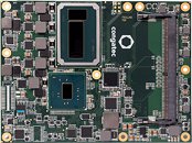
Source: AnandTech
Add your own comment

20 Comments on Intel Intros "Crystalwell" IGP Based Core "Skylake-R" Embedded CPUs

#1
TheinsanegamerN
Still waiting for any OEM to make a sub 15 inch iris pro laptop. At this point a unicorn would be more likely.
Posted on Reply
#2
RejZoR
I don't understand why eDRAM isn't used for compute on high end CPU's. Those few Skylakes with eDRAM showed some significant gains just because of it, but those CPU's are so underwhelming as a whole it doesn't even matter. But sticking eDRAM on a high end hexa or octa core, now that would be something.
Posted on Reply
#3
cdawall
where the hell are my stars
RejZoRI don't understand why eDRAM isn't used for compute on high end CPU's. Those few Skylakes with eDRAM showed some significant gains just because of it, but those CPU's are so underwhelming as a whole it doesn't even matter. But sticking eDRAM on a high end hexa or octa core, now that would be something.
Die size.
Posted on Reply
#5
hojnikb
Pls intel, bring iris iGPUs to desktop. HD550/580 in i3/i5 would be splendid.
Posted on Reply
#6
cdawall
where the hell are my stars
hojnikbPls intel, bring iris iGPUs to desktop. HD550/580 in i3/i5 would be splendid.
It will not fit inside of the package there is NOT room for that.
Posted on Reply
#7
hojnikb
cdawallIt will not fit inside of the package there is NOT room for that.
Is dualcore/HD550 die really that long ?
Posted on Reply
#8
cdawall
where the hell are my stars
hojnikbIs dualcore/HD550 die really that long ?
I'll illustrate why it wont happen

Posted on Reply
#9
TheinsanegamerN
cdawallI'll illustrate why it wont happen

They managed to make a desktop, socketed broadwell i7 with iris pro and a 128MB l4 cache, something tells me they could also do it with skylake. Literally, turn that GPU die 90 degrees and it would fit just fine.
Posted on Reply
#10
cdawall
where the hell are my stars
TheinsanegamerNThey managed to make a desktop, socketed broadwell i7 with iris pro and a 128MB l4 cache, something tells me they could also do it with skylake. Literally, turn that GPU die 90 degrees and it would fit just fine.
I could have sworn the 5775c was a substantially smaller gpu/edram die
Posted on Reply
#11
TheinsanegamerN
cdawallI could have sworn the 5775c was a substantially smaller gpu/edram die
Both had four CPU cores, and both had a 128MB l4 cache. The only real difference is that broadwell was only 48EU, while skylake is 72EU. And IIRC, the cache was significantly larger than the GPU was, so that still wouldnt make much of a difference. Look at the delidded 6700k, that die is much smaller than the iris pro one, so the GPU cant be that big, as a 24 core GPU fits into the CPU die.

Even with that skylake die, they could make it fit in a desktop chip. They would need to reorient the parts to be more square than rectangular, though.
Posted on Reply
#12
boogerlad
cdawallI'll illustrate why it wont happen

The gpu is still on the same die as the cpu.
Posted on Reply
#13
cdawall
where the hell are my stars
TheinsanegamerNBoth had four CPU cores, and both had a 128MB l4 cache. The only real difference is that broadwell was only 48EU, while skylake is 72EU. And IIRC, the cache was significantly larger than the GPU was, so that still wouldnt make much of a difference. Look at the delidded 6700k, that die is much smaller than the iris pro one, so the GPU cant be that big, as a 24 core GPU fits into the CPU die.

Even with that skylake die, they could make it fit in a desktop chip. They would need to reorient the parts to be more square than rectangular, though.
That last part is the issue... I guess we will see assuming price isn't dumb they are a nice a10 replacement

As for my labeling sorry should read edram for gpu I shouldn't make pictures while in class.
Posted on Reply
#14
PatBB
Your subject line is misleading, since these CPUs are not "embedded" in Intel terminology. Intel Desktop CPUs are divided into Consumer and Embedded CPU classes, the Consumer get released and discontinued whenever Intel feels like it, without notice. The Embedded CPUs have a guaranteed 7-year availability from Intel. Your subject line would be more accurate it you replaced "embedded" with the word "BGA".
Posted on Reply
#15
Tom.699
I'm missing something.
Can someone explain why this eDRAM is so big (physical size)?
For example Micron produces 8GBit DRAM chips that are in 9x13.2 mm BGA package (die itself is surely smaller).
8GBit is 8 times more memory than 128MB.
Also look at any regular 8GB or 16GB memory stick, memory chips are not so big.
Posted on Reply
#16
cadaveca
My name is Dave
Tom.699I'm missing something.
Can someone explain why this eDRAM is so big (physical size)?
For example Micron produces 8GBit DRAM chips that are in 9x13.2 mm BGA package (die itself is surely smaller).
8GBit is 8 times more memory than 128MB.
Also look at any regular 8GB or 16GB memory stick, memory chips are not so big.
The desktop memory is also no where near as fast.

Desktop DDR4 @ 3200 MHz = roughly 44000 MB/s. L3 cache on-chip with Skylake = 275 GB/s, going on 6x faster, with 11ns latency vs ~52ns latency on DDR4. The L4 cache is also connected "to the system" in a much different way.

AFAIK, the 2nd die is all cache, and the added execution units are inside the smaller chip (which is what makes the smaller chip larger than a standard desktop Skylake chip.
Posted on Reply
#17
HalfAHertz
cdawallI'll illustrate why it wont happen
The big die is actually the quad core CPU + 72 EU GPU and the small one is the L4 cache. They can't decouple the GPU from the CPU because they share resources...

On the desktop side, the standard configuration comes with 24 EUs and takes roughly ~50% of the die. Therefore we can extrapolate that the GPU in the 72EU part takes 75% of the die.

I have no idea why they chose to stack the two dies on top of each other instead of putting them parallel, side by side.
Posted on Reply
#18
Toothless
Tech, Games, and TPU!
Aaannndd will we see these priced around the APU range? (A10 series )

I want another tinybox desktop with this.
Posted on Reply
#19
cadaveca
My name is Dave
HalfAHertzThe big die is actually the quad core CPU + 72 EU GPU and the small one is the L4 cache. They can't decouple the GPU from the CPU because they share resources...

On the desktop side, the standard configuration comes with 24 EUs and takes roughly ~50% of the die. Therefore we can extrapolate that the GPU in the 72EU part takes 75% of the die.
I hear what you mean, but having de-lidded a few skylake chips now, the skylake die is very small, almost a bit smaller than the upper die shown in those images. It's roughly the size of a single memory IC, and to the right of the package is a sodimm slot for perspective. If you are right, and it's entirely possible you are, there must be more to Skylake-R. In the desktop CPU, CPU and GPU are connected via ringbus/L3. Perhaps this portion is also enlarged to accommodate connecting the added GPU EUs to the ringbus, or it could siply be that the package shown is smaller than the desktop skylake packages.
ToothlessAaannndd will we see these priced around the APU range? (A10 series )

I want another tinybox desktop with this.
Um, no, prices are listed in the OP, and are quite a bit more than what the A10-7890K APU costs.
Posted on Reply
#20
Aquinus
Resident Wat-man
I see a long compute die and a run of the mill Crystal Well IC on the picture in the op.

Compare that to a 4950HQ, the compute die is still very big compared to crystal well the only difference is that the compute cores have been elongated and made to be more rectangular than square. The picture in the OP seriously just looks like Skylake with Crystal Well slapped on (even if it's not as simple as merely "slapping it on".)
Posted on Reply
Add your own comment
Apr 28th, 2024 21:06 EDT change timezone

New Forum Posts

Popular Reviews

Controversial News Posts