Friday, May 3rd 2019

TSMC Expects Most 7nm Customers to Move to 6nm Density
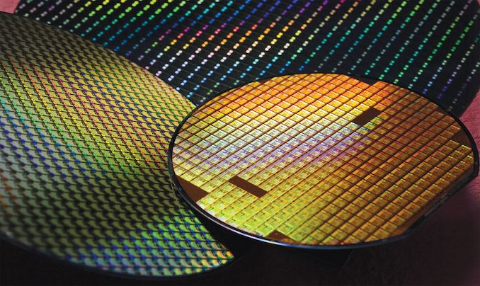
TSMC in its quarterly earnings call expressed confidence in that most of its 7 nm (N7) process production node customers would be looking to make the transition to their 6 nm (N6) process. In fact, the company expects that node to become the biggest target for volume ordering (and thus production) amongst its customers, since the new N6 fabrication technology will bring about a sort of "backwards compatibility" with design tools and semiconductor designs that manufacturers have already invested in for its N7 node, thus allowing for cost savings for its clients.
This is despite TSMC's N6 process being able to take advantage of extreme ultraviolet lithography (EUVL) to lower manufacturing complexity. This lowering is achieved by the fact that less exposures of the silicon are required for multi-patterning - which is needed today as TSMC's N7 uses solely deep ultraviolet (DUV) lithography. Interestingly, TSMC expects other clients to pick up its N7+ manufacturing node that aren't already using their 7nm node - the need to develop new tools and lesser design compatibility between its N7 and N7+ nodes compared no N7 and N6 being the justification. TSMC's N7+ will be the first node to leverage EUV, using up to four EUVL layers, while N6 expands it up to five layers, and the upcoming N5 cranks EUVL up to fourteen (allowing for 14 layers.)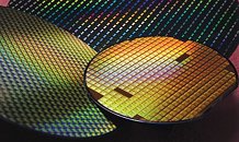
Source:
AnandTech
This is despite TSMC's N6 process being able to take advantage of extreme ultraviolet lithography (EUVL) to lower manufacturing complexity. This lowering is achieved by the fact that less exposures of the silicon are required for multi-patterning - which is needed today as TSMC's N7 uses solely deep ultraviolet (DUV) lithography. Interestingly, TSMC expects other clients to pick up its N7+ manufacturing node that aren't already using their 7nm node - the need to develop new tools and lesser design compatibility between its N7 and N7+ nodes compared no N7 and N6 being the justification. TSMC's N7+ will be the first node to leverage EUV, using up to four EUVL layers, while N6 expands it up to five layers, and the upcoming N5 cranks EUVL up to fourteen (allowing for 14 layers.)
9 Comments on TSMC Expects Most 7nm Customers to Move to 6nm Density
So 6nm Ryzen is definitely on the way
Remembers
Semiconductor Chip Sales Suffer Fourth Largest Decline in 35 Years
Backs out to main page
Yep that was the headline directly preceeding the current.
I wonder what they're going to say when they miss their targets by a mile.
I have to wonder...
At what point does H/W reliability drop off a cliff
with these ever finer resolutions???
Inquiring minds and all that...
I think things might get tough around sub 3nm nodes. Until then we will likely see 7>6>5>4>3 not big jumps like have seen so far from 28>16>14>12>7 etc.
EUV is supposed to change everything. 7nm+'s EUV is limited. 5nm is supposed to utilize EUV sufficiently. However TSMC seems not to believe 5nm since it announced and recommended 6nm after start of the 5nm's risk production.
Cost per transistor is decreasing. www.icknowledge.com/news/Technology%20and%20Cost%20Trends%20at%20Advanced%20Nodes%20-%20Revised.pdf
page 8
It claims 7nm has lower cost per unit but I don't think so. 7nm Vega is 1.6 times more dense than 14nm but the wafer cost is almost doubled from 16nm. I think 7nm's yield is not improved from 16/14nm.
iPhone's price is increasing edge.alluremedia.com.au/uploads/businessinsider/2018/09/BOM-v-price.jpg
browser.geekbench.com/ios-benchmarks
In single core, A12's improvement over A11 is 13%. A11 : A10 is 26%. A10 : A9 is 52%
In multi core, A12 : A11 is 10%. A11 : A10 is 76%. A10 : A9 is 46%.