News Posts matching #EUV

Return to Keyword Browsing

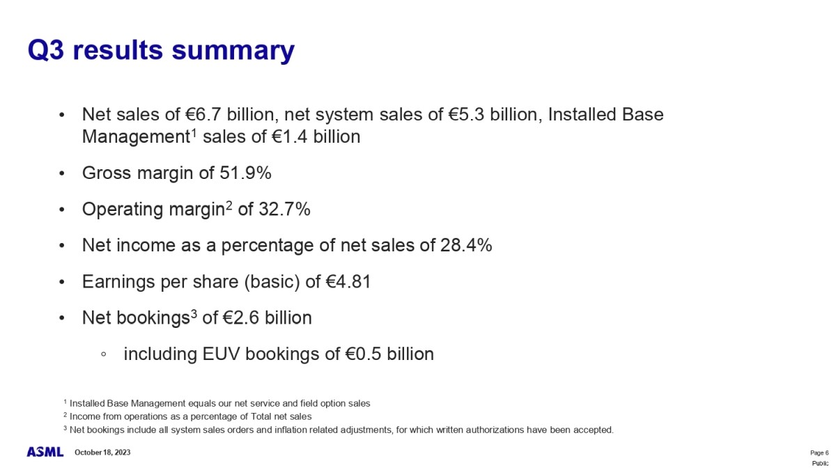
ASML reports €5.3 billion total net sales and €1.2 billion net income in Q1 2024

Today, ASML Holding NV (ASML) has published its 2024 first-quarter results.
  • Q1 total net sales of €5.3 billion, gross margin of 51.0%, net income of €1.2 billion
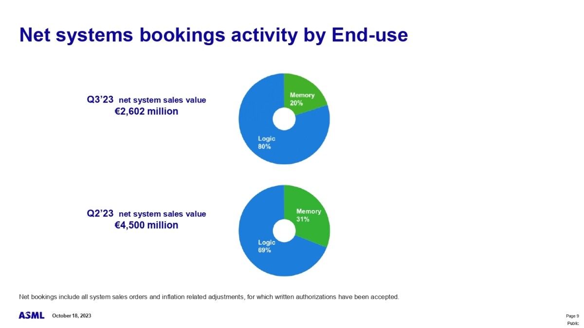
  • Quarterly net bookings in Q1 of €3.6 billion of which €656 million is EUV
  • ASML expects Q2 2024 total net sales between €5.7 billion and €6.2 billion, and a gross margin between 50% and 51%
  • ASML expects 2024 total net sales to be similar to 2023
CEO statement and outlook
"Our first-quarter total net sales came in at €5.3 billion, at the midpoint of our guidance, with a gross margin of 51.0% which is above guidance, primarily driven by product mix and one-offs. We expect second-quarter total net sales between €5.7 billion and €6.2 billion with a gross margin between 50% and 51%. ASML expects R&D costs of around €1,070 million and SG&A costs of around €295 million. Our outlook for the full year 2024 is unchanged, with the second half of the year expected to be stronger than the first half, in line with the industry's continued recovery from the downturn. We see 2024 as a transition year with continued investments in both capacity ramp and technology, to be ready for the turn in the cycle," said ASML President and Chief Executive Officer Peter Wennink.

Intel Lunar Lake Chiplet Arrangement Sees Fewer Tiles—Compute and SoC

Intel Core Ultra "Lunar Lake-MX" will be the company's bulwark against Apple's M-series Pro and Max chips, designed to power the next crop of performance ultraportables. The MX codename extension denotes MoP (memory-on-package), which sees stacked LPDDR5X memory chips share the package's fiberglass substrate with the chip, to conserve PCB footprint, and give Intel greater control over the right kind of memory speed, timings, and power-management features suited to its microarchitecture. This is essentially what Apple does with its M-series SoCs powering its MacBooks and iPad Pros. Igor's Lab scored the motherlode on the way Intel has restructured the various components across its chiplets, and the various I/O wired to the package.

When compared to "Meteor Lake," the "Lunar Lake" microarchitecture sees a small amount of "re-aggregation" of the various logic-heavy components of the processor. On "Meteor Lake," the CPU cores and the iGPU sat on separate tiles—Compute tile and Graphics tile, respectively, with a large SoC tile sitting between them, and a smaller I/O tile that serves as an extension of the SoC tile. All four tiles sat on top of a Foveros base tile, which is essentially an interposer—a silicon die that facilitates high-density microscopic wiring between the various tiles that are placed on top of it. With "Lunar Lake," there are only two tiles—the Compute tile, and the SoC tile.

TSMC 3nm Node to Make 20% of Company's Revenues in 2024

The 3 nm EUV node, which will be TSMC's final semiconductor fabrication node to implement FinFET transistors, will make for a staggering 20% of TSMC's revenues in 2024, a report by ICSmart says. 20% is big for a new foundry node, considering that TSMC is simultaneously running 4 nm and 5 nm EUV nodes; 6 nm and 7 nm DUV nodes; and several older mature nodes. Apple is expected to be the foundry's biggest customer for 3 nm, as it could power the company's current A17 and M3, and upcoming A18 and M4 line of chips for its next-generation iPhone and MacBooks; followed by NVIDIA, AMD, and possibly even Intel. AMD is expected to build some versions of its upcoming "Zen 5" processors on 3 nm; while Intel is expected to use 3 nm for some of the tiles of its upcoming "Lunar Lake" processor. The same report goes to suggest that 3 nm will make up 30% of TSMC's revenues in 2025.

Huawei and SMIC Prepare Quadruple Semiconductor Patterning for 5 nm Production

According to Bloomberg's latest investigation, Huawei and Semiconductor Manufacturing International Corporation (SMIC) have submitted patents on the self-aligned quadruple patterning (SAQP) pattern etching technique to enable SMIC to achieve 5 nm semiconductor production. The two Chinese giants have been working with the Deep Ultra Violet (DUV) machinery to develop a pattern etching technique allowing SMIC to produce a node compliant with the US exporting rules while maintaining the density improvements from the previously announced 7 nm node. In the 7 nm process, SMIC most likely used self-aligned dual patterning (SADP) with DUV tools, but for the increased density of the 5 nm node, a doubling to SAQP is required. In semiconductor manufacturing, lithography tools take multiple turns to etch the design of the silicon wafer.

Especially with smaller nodes getting ever-increasing density requirements, it is becoming challenging to etch sub-10 nm designs using DUV tools. That is where Extreme Ultra Violet (EUV) tools from ASML come into play. With EUV, the wavelengths of the lithography printers are 14 times smaller than DUV, at only 13.5 nm, compared to 193 nm of ArF immersion DUV systems. This means that without EUV, SMIC has to look into alternatives like SAQP to increase the density of its nodes and, as a result, include more complications and possibly lower yields. As an example, Intel tried to use SAQP in its first 10 nm nodes to reduce reliance on EUV, which resulted in a series of delays and complications, eventually pushing Intel into EUV. While Huawei and SMIC may develop a more efficient solution for SAQP, the use of EUV is imminent as the regular DUV can not keep up with the increasing density of semiconductor nodes. Given that ASML can't ship its EUV machinery to China, Huawei is supposedly developing its own EUV machines, but will likely take a few more years to show.

ASML Celebrates First Installation of Twinscan NXE:3800E Low-NA EUV Litho Tool

ASML celebrated an important milestone last week—the company's social media account shared news about their third generation extreme ultraviolet (EUV) lithography tool reaching an unnamed customer: "chipmakers have a need for speed! The first Twinscan NXE:3800E is now being installed in a chip fab. 🔧 With its new wafer stages, the system will deliver leading edge productivity for printing advanced chips. We're pushing lithography to new limits." The post included a couple of snaps—ASML workers were gathered in front of a pair of climatized containers, and Peter Wennink (President and CEO) and Christophe Fouquet (EVP and CBO) thanked staff at company HQ.

The Twinscan NXE:3800E is ASML's latest platform from a series of 0.33 numerical aperture (Low-NA) lithography scanners. Information is scarce—the company has not yet published a 3800E product page. The preceding model—Twinscan NXE:3600D—supports EUV volume production at 3 and 5 nm. ASML roadmaps imply that the Twinscan NXE:3800E has been designed to produce chips on 2 and 3 nm-class technologies. The company's cutting-edge High-NA extreme ultraviolet (EUV) chipmaking tools (High-NA Twinscan EXE) are expected to cost around $380 million—reports from last month point to a possible $183 million price point for "existing Low-NA EUV lithography systems." Another Low-NA EUV machine is reported to be lined up for a possible 2026 release window—ASML's next-gen Twinscan NXE:4000F model will co-exist alongside emerging (pricier) High-NA solutions.

Silicon Motion Unveils 6nm UFS 4.0 Controller for AI Smartphones, Edge Computing and Automotive Applications

Silicon Motion Technology Corporation ("Silicon Motion"), a global leader in designing and marketing NAND flash controllers for solid state storage devices, today introduced its UFS (Universal Flash Storage) 4.0 controller, the SM2756, as the flagship of the industry's broadest merchant portfolio of UFS controller solutions for the growing requirements of AI-powered smartphones as well as other high-performance applications including automotive and edge computing. The company also added a new, second generation SM2753 UFS 3.1 controller to broaden its portfolio of controllers now supporting UFS 4.0 to UFS 2.2 standards. Silicon Motion's UFS portfolio delivers high-performance and low power embedded storage for flagship to mainstream and value mobile and computing devices, supporting the broadest range of NAND flash, including next-generation high speed 3D TLC and QLC NAND.

The new SM2756 UFS 4.0 controller solution is the world's most advanced controller, built on leading 6 nm EUV technology and using MIPI M-PHY low-power architecture, providing the right balance of high performance and power efficiency to enable the all day computing needs of today's premium and AI mobile devices. The SM2756 achieves sequential read performance exceeding 4,300 MB/s and sequential write speeds of over 4,000 MB/s and supports the broadest range of 3D TLC and QLC NAND flash with densities of up to 2 TB.

Intel 14A Node Delivers 15% Improvement over 18A, A14-E Adds Another 5%

Intel is revamping its foundry play, and the company is set on its goals of becoming a strong contender to rivals such as TSMC and Samsung. Under Pat Gelsinger's lead, Intel recently split (virtually, under the same company) its units into Intel Product and Intel Foundry. During the SPIE 2024 conference for optics and photonics, Anne Kelleher, Intel's senior vice president, revealed that the 14A (1.4 nm) process offers a 15% performance-per-watt improvement over the company's 18A (1.8 nanometers) process. Additionally, the enhanced 14A-E process boasts a further 5% performance boost from the regular A14 node, being a small refresh. Intel's 14A process is set to be the first to utilize High-NA extreme ultraviolet (EUV) equipment, delivering a 20% increase in transistor logic density compared to the 18A node.

The company's aggressive pursuit of next-generation processes poses a significant threat to Samsung Electronics, which currently holds the second position in the foundry market. As part of its IDM 2.0 strategy, Intel hopes to reclaim its position as a leading foundry player and surpass Samsung by 2030. The company's collaboration with American companies, such as Microsoft, further solidifies its ambitions. Intel has already secured a $15 billion chip production contract with Microsoft for its 1.8 nm 18A process. The semiconductor industry is closely monitoring Intel's progress, as the company's advancements in process technology could potentially reshape the competitive landscape. With Samsung planning to mass-produce 2 nm process products next year, the race for dominance in the foundry market is heating up.

SMIC Prepares for 3 nm Node Development, Requires Chinese Government Subsidies

SMIC, China's largest semiconductor manufacturer, is reportedly assembling a dedicated team to develop 3 nm semiconductor node technology, following reports of the company setting up 5 nm chip production for Huawei later this year. This move is part of SMIC's efforts to achieve independence from foreign companies and reduce its reliance on US technology. According to a report from Joongang, SMIC's initial goal is to commence operations of its 5 nm production line, which will mass-produce Huawei chipsets for various products, including AI silicon. However, SMIC is already looking beyond the 5 nm node. The company has assembled an internal research and development team to begin work on the next-generation 3 nm node.

The Chinese manufacturer is expected to accomplish this using existing DUV machinery, as ASML, the sole supplier of advanced EUV technology, is prohibited from providing equipment to Chinese companies due to US restrictions. It is reported that one of the biggest challenges facing SMIC is the potential for low yields and high production costs. The company is seeking substantial subsidies from the Chinese government to overcome these obstacles. Receiving government subsidies will be crucial for SMIC, especially considering that its 5 nm chips are expected to be up to 50 percent more expensive than TSMC's due to the use of older DUV equipment. The first 3 nm wafers from SMIC are not expected to roll out for several years, as the company will prioritize the commercialization of Huawei's 5 nm chips. This ambitious undertaking by SMIC represents a significant challenge for the company as it strives to reduce its dependence on foreign semiconductor technology and establish itself as an essential player in the global manufacturing industry.

ASML's Future Growth in Netherlands Uncertain Amid Immigration Concerns

Chipmaking manufacturing equipment giant ASML has expressed concerns about staying in the Netherlands and considering expansion into other countries due to its home country's capped possibilities. On Wednesday, ASML executives met with Netherlands Prime Minister Mark Rutte to discuss the company's growth plans. The meeting, however, failed to fully resolve ASML's concerns surrounding the country's stance on skilled foreign labor, leaving uncertainty over the tech giant's expansion in its home market. Being one of the world's largest suppliers to chipmakers, ASML has said it needs to double its operations in the following decade to meet soaring demand. However, the company is hitting roadblocks in the Netherlands, including difficulty obtaining building permits, constraints on the electrical grid, transportation bottlenecks, and a need for supporting infrastructure like hospitals, schools, and housing. A key issue is the Netherlands' ability to attract scarce foreign engineering talent, with over 40% of ASML's Dutch workforce being non-Dutch. Recent parliamentary motions to cap international students and scrap a tax break for skilled migrants have met with criticism from ASML and other tech employers.

In an effort dubbed "Operation Beethoven," the Dutch government is scrambling to address ASML's concerns and prevent the company from expanding abroad, having already seen multinationals like Shell and Unilever leave their home country in recent years. However, ASML CEO Peter Wennink said that while the company prefers to grow in the Netherlands, it can do so elsewhere if needed. The situation comes amid pressure from the US for allies like the Netherlands to tighten restrictions on China's further access to semiconductor technology. As the sole producer of extreme ultraviolet (EUV) lithography machines crucial for advanced chipmaking, like High-NA and Low-NA, ASML holds strategic importance beyond just economics. With a new right-wing Dutch government being formed, whether a compromise can be reached to ensure ASML's continued growth in the Netherlands remains to be seen. The tech giant's decision could significantly affect the Dutch economy and its position in the global chip industry.

Samsung Bags 2 nm Wafer Order from Japanese AI Chip Startup

Samsung Electronics foundry has reportedly bagged a mass production order for its cutting edge 2 nm EUV foundry node from Japanese AI chip startup PFN (Preferred Networks). This is reportedly the first major third party order for the 2 nm node. Founded in 2014, PFN specializes in AI and IoT chips, and spun off from Preferred Infrastructure. Samsung's 2 nm node, called the SF2, is on track for delivery of mass produced chips in 2025, which means much of 2024 will be spent on testing, validation, and risk production, with the node expected to go live toward the end of the year. Samsung SF2 is being designed to offer 25% higher power efficiency (at iso-clocks), and 12% increase in performance, over SF3 (3 nm EUV FinFET). In the semiconductor fabrication market, Samsung SF2 competes against TSMC N2 and Intel 20A.

Report: Intel Seeks $2 Billion in Funding for Ireland Fab 34 Expansion

According to a Bloomberg report, Intel is seeking to raise at least $2 billion in equity funding from investors for expanding its fabrication facility in Leixlip, Ireland, known as Fab 34. The chipmaker has hired an advisor to find potential investors interested in providing capital for the project. Fab 34 is currently Intel's only chip plant in Europe that uses cutting-edge extreme ultraviolet (EUV) lithography. It produces processors on the Intel 4 process node, including compute tiles for Meteor Lake client CPUs and expected future Xeon data center chips. While $2 billion alone cannot finance the construction of an entirely new fab today, it can support meaningful expansion or upgrades of existing capacity. Intel likely aims to grow Fab 34's output and/or transition it to more advanced 3 nm-class technologies like Intel 3, Intel 20A, or Intel 18A.

Expanding production aligns with Intel's needs for its own products and its Intel Foundry Services business, providing contract manufacturing. Intel previously secured a $15 billion investment from Brookfield Infrastructure for its Arizona fabs in exchange for a 49% stake, demonstrating the company's willingness to partner to raise capital for manufacturing projects. The Brookfield deal also set a precedent of using outside financing to supplement Intel's own spending budget. It provided $15 billion in effectively free cash flow Intel can redirect to other priorities like new fabs without increasing debt. Intel's latest fundraising efforts for the Ireland site follow a similar equity investment model that leverages outside capital to support its manufacturing expansion plans. Acquiring High-NA EUV machinery for manufacturing is costly, as these machines can reach up to $380 million alone.

ASML High-NA EUV Twinscan EXE Machines Cost $380 Million, 10-20 Units Already Booked

ASML has revealed that its cutting-edge High-NA extreme ultraviolet (EUV) chipmaking tools, called High-NA Twinscan EXE, will cost around $380 million each—over twice as much as its existing Low-NA EUV lithography systems that cost about $183 million. The company has taken 10-20 initial orders from the likes of Intel and SK Hynix and plans to manufacture 20 High-NA systems annually by 2028 to meet demand. The High-NA EUV technology represents a major breakthrough, enabling an improved 8 nm imprint resolution compared to 13 nm with current Low-NA EUV tools. This allows chipmakers to produce transistors that are nearly 1.7 times smaller, translating to a threefold increase in transistor density on chips. Attaining this level of precision is critical for manufacturing sub-3 nm chips, an industry goal for 2025-2026. It also eliminates the need for complex double patterning techniques required presently.

However, superior performance comes at a cost - literally and figuratively. The hefty $380 million price tag for each High-NA system introduces financial challenges for chipmakers. Additionally, the larger High-NA tools require completely reconfiguring chip fabrication facilities. Their halved imaging field also necessitates rethinking chip designs. As a result, adoption timelines differ across companies - Intel intends to deploy High-NA EUV at an advanced 1.8 nm (18A) node, while TSMC is taking a more conservative approach, potentially implementing it only in 2030 and not rushing the use of these lithography machines, as the company's nodes are already developing well and on time. Interestingly, the installation process of ASML's High-NA Twinscan EXE 150,000-kilogram system required 250 crates, 250 engineers, and six months to complete. So, production is as equally complex as the installation and operation of this delicate machinery.

Canon Wants to Challenge ASML with a Cheaper 5 nm Nanoimprint Lithography Machine

Japanese tech giant Canon hopes to shake up the semiconductor manufacturing industry by shipping new low-cost nanoimprint lithography (NIL) machines as early as this year. The technology, which stamps chip designs onto silicon wafers rather than using more complex light-based etching like market leader ASML's systems, could allow Canon to undercut rivals and democratize leading-edge chip production. "We would like to start shipping this year or next year...while the market is hot. It is a very unique technology that will enable cutting-edge chips to be made simply and at a low cost," said Hiroaki Takeishi, head of Canon's industrial group overseeing nanoimprint lithography technological advancement. Nanoimprint machines target a semiconductor node width of 5 nanometers, aiming to reach 2 nm eventually. Takeishi said the technology has primarily resolved previous defect rate issues, but success will depend on convincing customers that integration into existing fabrication plants is worthwhile.

There is skepticism about Canon's ability to significantly disrupt the market led by ASML's expensive but sophisticated extreme ultraviolet (EUV) lithography tools. However, if nanoimprint can increase yields to nearly 90% at lower costs, it could carve out a niche, especially with EUV supply struggling to meet surging demand. Canon's NIL machines are supposedly 40% the cost of ASML machinery, while operating with up to 90% lower power draw. Initially focusing on 3D NAND memory chips rather than complex processors, Canon must contend with export controls limiting sales to China. But with few options left, Takeishi said Canon will "pay careful attention" to sanctions risks. If successfully deployed commercially after 15+ years in development, Canon's nanoimprint technology could shift the competitive landscape by enabling new players to manufacture leading-edge semiconductors at dramatically lower costs. But it remains to be seen whether the new machines' defect rates, integration challenges, and geopolitical headwinds will allow Canon to disrupt the chipmaking giants it aims to compete with significantly.

Intel Reports Fourth-Quarter and Full-Year 2023 Financial Results

Intel Corporation today reported fourth-quarter and full-year 2023 financial results. "We delivered strong Q4 results, surpassing expectations for the fourth consecutive quarter with revenue at the higher end of our guidance," said Pat Gelsinger, Intel CEO. "The quarter capped a year of tremendous progress on Intel's transformation, where we consistently drove execution and accelerated innovation, resulting in strong customer momentum for our products. In 2024, we remain relentlessly focused on achieving process and product leadership, continuing to build our external foundry business and at-scale global manufacturing, and executing our mission to bring AI everywhere as we drive long-term value for stakeholders."

David Zinsner, Intel CFO, said, "We continued to drive operational efficiencies in the fourth quarter, and comfortably achieved our commitment to deliver $3 billion in cost savings in 2023. We expect to unlock further efficiencies in 2024 and beyond as we implement our new internal foundry model, which is designed to drive greater transparency and accountability and higher returns on our owners' capital." For the full year, the company generated $11.5 billion in cash from operations and paid dividends of $3.1 billion.

More AMD Ryzen 9000 "Zen 5" Desktop Processor Details Emerge

AMD is looking to debut its Ryzen 9000 series "Granite Ridge" desktop processors based on the "Zen 5" microarchitecture some time around May-June 2024, according to High Yield YT, a reliable source with AMD leaks. These processors will be built in the existing Socket AM5 package, and be compatible with all existing AMD 600 series chipset motherboards. It remains to be seen if AMD debuts a new line of motherboard chipsets. Almost all Socket AM5 motherboards come with the USB BIOS flashback feature, which means motherboards from even the earliest production batches that are in the retail channel, should be able to easily support the new processors.

AMD is giving its next-gen desktop processors the Ryzen 9000 series processor model numbering, as it used the Ryzen 8000 series for its recently announced Socket AM5 desktop APUs based on the "Hawk Point" monolithic silicon. "Granite Ridge" will be a chiplet-based processor, much like the Ryzen 7000 series "Raphael." In fact, it will even retain the same 6 nm client I/O die (cIOD) as "Raphael," with some possible revisions made to increase its native DDR5 memory frequency (up from the current DDR5-5200), and improve its memory overclocking capabilities. It's being reported that DDR5-6400 could be the new "sweetspot" memory speed for these processors, up from the current DDR5-6000.

ASML reports €27.6 Billion Net Sales and €7.8 Billion Net Income in 2023

Today, ASML Holding NV (ASML) has published its 2023 fourth quarter and full-year results.
  • Q4 net sales of €7.2 billion, gross margin of 51.4%, net income of €2.0 billion
  • Quarterly net bookings in Q4 of €9.2 billion of which €5.6 billion is EUV
  • 2023 net sales of €27.6 billion, gross margin of 51.3%, net income of €7.8 billion
  • ASML expects 2024 net sales to be similar to 2023
  • ASML expects Q1 2024 net sales between €5.0 billion and €5.5 billion and a gross margin between 48% and 49%
CEO statement and outlook
"Our fourth-quarter net sales came in at €7.2 billion with a gross margin of 51.4%, both slightly above our guidance. ASML achieved another strong year in 2023 with 30% growth, ending with total net sales for the year of €27.6 billion, a gross margin of 51.3% and a backlog of €39 billion. We shipped the first modules of the first High NA EUV system, EXE:5000, to a customer before the end of the year."

Not Just TSMC, Even Samsung Running Behind Schedule with its U.S. Fab

Delays in the construction of its U.S. based semiconductor fab may have just cost the Chairman of TSMC his job, but the Koreans aren't faring any better. BusinessKorea reports that Samsung Electronics has pushed the timeline for mass-production in its upcoming Austin Texas-based fab to 2025. Its construction was originally slated to be complete by now, with risk production and testing through early 2024, and mass production later in the year, which has all been pushed to 2025. The company now hopes to push its first wafer toward the end of 2024, with mass production expected some time in 2025.

Samsung reportedly blames issues with U.S. Government subsidies and regulatory problems behind the delays. A key aspect of getting cutting edge Asian foundries such as TSMC and Samsung to invest in the U.S. had to do with government subsidies to help these fabs overcome the uphill task of doing so Stateside and making the venture profitable. The U.S. had a sense of urgency in bringing these companies over, as it saw a potential conflict across the Taiwan straits, which threatened to disrupt practically the entire global digital economy. The company's first production line in this foundry was expected to be 4 nm EUV FinFET. It remains to be seen just how relevant and cutting edge 4 nm EUV is in 2025, as both TSMC and Intel hope to have Nanosheet transistors and nodes such as the TSMC N2 and Intel 20A taking shape by then.

DNP Develops Photomask Process for 3nm EUV Lithography

Dai Nippon Printing Co., Ltd. (DNP) has successfully developed a photomask manufacturing process capable of accommodating the 3-nanometer (10-9 meter) lithography process that supports Extreme Ultra-Violet (EUV) lithography, the cutting-edge process for semiconductor manufacturing.

Background
DNP has continually responded to the demands of semiconductor manufacturers in terms of performance and quality. In 2016, we became the world's first merchant photomask manufacturer to introduce the multi-beam mask writing tool (MBMW). In 2020, we developed a photomask manufacturing process for 5 nm EUV lithography processes, and have been supplying masks that meet the needs of the semiconductor market. In this latest development, in order to meet the needs of further miniaturization, we have developed a photomask for EUV lithography capable of supporting 3 nm processes.

Sony PlayStation 5 Pro Packs an Updated RDNA3 GPU with 60 CU

Sony is developing the PlayStation 5 Pro console that targets higher refresh-rate gaming at 4K Ultra HD, or higher in-game eye-candy, given its faster hardware. Details about the console are few and far between, given its late-2024 tentative release, but by now the company would have co-developed its semi-custom SoC, so it could spend the next year extensively testing and optimizing it, before mass production in the 2-3 quarters leading up to the launch. Kepler_L2 and Tom Henderson on Twitter are fairly reliable sources for PlayStation hardware leaks, and piecing their recent posts together, VideoCardz compiled the most probable specs of the SoC at the heart of the PlayStation 5 Pro.

The semi-custom SoC powering the PlayStation 5 Pro is co-developed by Sony Computer Entertainment (SCE) and AMD; and is codenamed "Viola." The monolithic chip is built on the TSMC N4P foundry node (4 nm EUV), which is a big upgrade from the 7 nm DUV node on which the "Oberon" SoC powering the original PlayStation 5, and 6 nm DUV node powering the "Oberon Plus" SoC of the refreshed PS5, are based on. Sony is leaving the CPU component largely untouched, it is an 8-core/16-thread unit based on the "Zen 2" microarchitecture, spread across two 4-core CCXs. The CPU has a maximum boost frequency of 4.40 GHz, dialed up from the 3.50 GHz maximum boost of "Oberon." The iGPU is where all the magic happens.

AMD Ryzen 8040 Series "Hawk Point" Mobile Processors Announced with a Faster NPU

AMD today announced the new Ryzen 8040 mobile processor series codenamed "Hawk Point." These chips are shipping to notebook manufacturers now, and the first notebooks powered by these should be available to consumers in Q1-2024. At the heart of this processor is a significantly faster neural processing unit (NPU), designed to accelerate AI applications that will become relevant next year, as Microsoft prepares to launch Windows 12, and software vendors make greater use of generative AI in consumer applications.

The Ryzen 8040 "Hawk Point" processor is almost identical in design and features to the Ryzen 7040 "Phoenix," except for a faster Ryzen AI NPU. While this is based on the same first-generation XDNA architecture, its NPU performance has been increased to 16 TOPS, compared to 10 TOPS of the NPU on the "Phoenix" silicon. AMD is taking a whole-of-silicon approach to AI acceleration, which includes not just the NPU, but also the "Zen 4" CPU cores that support the AVX-512 VNNI instruction set that's relevant to AI; and the iGPU based on the RDNA 3 graphics architecture, with each of its compute unit featuring two AI accelerators, components that make the SIMD cores crunch matrix math. The whole-of-silicon performance figures for "Phoenix" is 33 TOPS; while "Hawk Point" boasts of 39 TOPS. In benchmarks by AMD, "Hawk Point" is shown delivering a 40% improvement in vision models, and Llama 2, over the Ryzen 7040 "Phoenix" series.

ASML Supervisory Board Intends to Appoint Christophe Fouquet as President and CEO

Today the Supervisory Board of ASML Holding NV (ASML) announces that it intends to appoint Christophe Fouquet, currently ASML's Chief Business Officer and member of the Board of Management, as the company's next President and Chief Executive Officer. The appointment is subject to notification of the Annual General Meeting of Shareholders on April 24, 2024. On the same date, ASML's Co-Presidents Peter Wennink and Martin van den Brink will retire from ASML upon completion of their current appointment terms.

Nils Andersen, Chairman of the Supervisory Board, said: "The Supervisory Board, together with the management team, has gone through a comprehensive succession planning process. With Christophe, we have identified a very experienced leader with deep understanding of ASML's technology and the semiconductor industry ecosystem - acquired through different roles at ASML and other companies - and the right leadership qualities and culture fit. We are grateful and full of admiration for the immense contributions that Peter and Martin have made over decades, helping to shape ASML into the successful company that it is today. Peter and Martin have been preparing ASML for the future, and we know they will be fully engaged in securing a smooth transition for the company and all of ASML's stakeholders."

Rapidus and Tenstorrent Partner to Accelerate Development of AI Edge Device Domain Based on 2 nm Logic

Rapidus Corporation, a company involved in the research, development, design, manufacture, and sales of advanced logic semiconductors, today announced an agreement with Tenstorrent Inc., a next-generation computing company building computers for AI, to jointly develop semiconductor IP (design assets) in the field of AI edge devices based on 2 nm logic semiconductors.

In addition to its AI processors and servers, Tenstorrent built and owns the world's most performant RISC-V CPU IP and licenses that technology to its customers around the world. Through this technological partnership with Rapidus, Tenstorrent will accelerate the development of cutting-edge devices to meet the needs of the ever-evolving digital society.

ASML Reports €6.7 Billion Net Sales and €1.9 Billion Net Income in Q3 2023

Today ASML Holding NV (ASML) has published its 2023 third-quarter results.
  • Q3 net sales of €6.7 billion, gross margin of 51.9%, net income of €1.9 billion
  • Quarterly net bookings in Q3 of €2.6 billion of which €0.5 billion is EUV
  • ASML expects Q4 2023 net sales between €6.7 billion and €7.1 billion and a gross margin between 50% and 51%
  • ASML confirms its expectation to grow net sales towards 30% in 2023
CEO statement and outlook
"Our third-quarter net sales came in at €6.7 billion, around the midpoint of our guidance, with a gross margin of 51.9%, higher than guided, primarily driven by the DUV product mix and some one-off costs effects. "The semiconductor industry is currently working through the bottom of the cycle and our customers expect the inflection point to be visible by the end of this year. Customers continue to be uncertain about the shape of the demand recovery in the industry. We therefore expect 2024 to be a transition year. Based on our current perspective, we take a more conservative view and expect a revenue number similar to 2023. But we also look at 2024 as an important year to prepare for significant growth that we expect for 2025.

More AMD "Strix Point" Mobile Processor Details Emerge

"Strix Point" is the codename for AMD's next-generation mobile processor succeeding the current Ryzen 7040 series "Phoenix." More details of the processor emerged thanks to "All The Watts!!" on Twitter. The CPU of "Strix Point" will be heterogenous, in that it will feature two different kinds of CPU cores, but with essentially the same ISA and IPC. It is rumored that the processor will feature 4 "Zen 5" CPU cores, and 8 "Zen 5c" cores.

Both core types feature an identical IPC, but the "Zen 5" cores can hold onto higher boost frequencies, and have a wider frequency band, than the "Zen 5c" cores. From what we can deduce from the current "Zen 4c" cores, "Zen 5c" cores aren't strictly "efficiency" cores, as they still offer the full breadth of core ISA as "Zen 5," including SMT. In its maximum configuration, "Strix Point" will hence be a 12-core/24-thread processor. The two CPU core types sit in two different CCX (CPU core complexes), the "Zen 5" CCX has 4 cores sharing a 16 MB L3 cache, while the "Zen 5c" CCX shares a 16 MB L3 cache among 8 cores. AMD will probably use a software-based solution to ensure the right kind of workload from the OS is processed by the right kind of CPU core.

Intel to Start High-Volume EUV Production in Ireland, Intel 4 Node Enters Mass-production

Intel Foundry Services (IFS) today announced that it will commence mass-production on its first silicon fabrication node that leverages extreme ultraviolet (EUV) lithography, Intel 4. On September 29, the Intel 4 node will start rolling at the company's facility in Leixlip, Ireland, dubbed Fab 34. CEO Pat Gelsinger, Dr. Ann Kelleher, general manager of Technology Development at Intel, and Keyvan Esfarjani, chief global operations officer, will be present at a ceremony commemorating production of the first wafers.

Intel 4 is an advanced foundry that leverages EUV, and offers both transistor densities and electrical characteristics comparable to TSMC's 5 nm-class and 4 nm-class foundry nodes. Among the first chips to be built are the compute tiles of the company's Core "Meteor Lake" processors, which contain their next-generation CPU cores. Compared to the current Intel 7 node, Intel 4 offers double the area scaling for logic libraries, a 20% iso-power improvement, and introduces the new metal-insulator-metal (MIM) capacitor.
Return to Keyword Browsing
Apr 23rd, 2024 16:43 EDT change timezone

New Forum Posts

Popular Reviews

Controversial News Posts