News Posts matching #Taiwan

Return to Keyword Browsing

NVIDIA May Cut TSMC Chip Orders Amid Mounting Pressure, Report Claims

NVIDIA may be slowing down its chip orders at TSMC, according to a new report from Taiwan's Commercial Times. The outlet cites unnamed supply chain sources but doesn't name a product, node, size, or timeline. Neither NVIDIA nor TSMC have commented so far, and the claims are single-sourced for now. The report frames this as NVIDIA being squeezed from inside and out. On the inside, there's Jensen Huang's November 8 email to staff, in which he apologized for an extramarital affair, and the board's independent investigation into reports that he was targeted by a foreign intelligence effort. The board has said it has no reason to believe national security or NVIDIA secrets were compromised.

The outside pressure mostly comes down to export controls. The report points to tighter export reviews and H200 chips reportedly stockpiled in Hong Kong, both of which it says raise the risk of NVIDIA scaling back orders. It also cites foreign media reports suggesting that some firms approved to handle H200 could be shell companies, which feeds concerns that chips might reach China through fronts like these or middlemen in other countries. The report presents that as a suspicion rather than a finding, and if cuts do happen, upstream suppliers such as TSMC and ASE are the most exposed.

Terafab Wants to Become One of the Largest Memory Makers by 2032

According to Nikkei, a procurement team from Terafab, the chip venture between Tesla and SpaceX, visited Japan and walked local equipment makers through what it plans to buy. The targets it reportedly shared are gigantic: 1 million wafers per month from 2032 onward, with around 700,000 of those going to memory chips and 300,000 to logic. Nikkei's headline puts that at 40 times the output of Japan's Rapidus. The same split first surfaced in a Jiji Press report last month, which said a single Texas plant would handle both memory and logic, with a pilot fab completed as early as July 2027. Intel is reportedly helping with logic using its 2 nm and 1.4 nm-class technology, while a Taiwanese company has been floated as a technology partner for memory. That could be Nanya, though nothing is confirmed.

For context, Samsung's entire DRAM output was estimated at 650,000 to 700,000 wafers a month late last year, while SK hynix was at about 550,000 earlier this year and hopes to reach roughly 1 million by 2030 or 2031. It isn't clear whether Terafab's memory figure covers DRAM alone or also includes NAND, so the Samsung comparison is a loose one. Musk has also been careful with his own dates. On an October SpaceX call, he put "big error bars" on reaching volume production by Q3 2028, with a first SRAM test chip planned for mid-2027 at Terafab's Austin research lab.

TSMC Could Charge Up to 20% More for CoWoS Packaging Amid AI Crunch

TSMC is reportedly considering raising prices for its CoWoS (Chip on Wafer on Substrate) advanced packaging by as much as 20%, according to supply chain sources cited by Taiwan's Commercial Times. Foundries and outsourced packaging firms are apparently weighing another round of 10% to 20% increases, as CoWoS demand has spread beyond AI GPUs to server CPUs and custom ASICs, leaving a growing backlog of unfilled orders. TSMC hasn't confirmed anything yet.

Testing is turning into a bottleneck of its own. Nomura estimates, via Seoul Economic Daily, that NVIDIA's Blackwell takes roughly four times longer than Hopper in final testing, while Rubin could need seven times as long. Packages keep growing too, with TSMC already mass producing CoWoS-L at 5.5 times the reticle limit. Tool lead times have reportedly stretched from three to six months to as long as eight months. TSMC, which usually negotiates for discounts or extra features, apparently placed this year's equipment orders at existing prices instead, which says a lot about how tight things are.

TSMC A14 Node to Break Eight Years of SRAM Scaling Stagnation

TSMC, the world's largest and most advanced semiconductor manufacturer, has been grappling with stagnant progress in SRAM scaling for years. Since the launch of the N5 5 nm process in 2020, the size of the SRAM 6T bitcell has remained around 0.021 µm². While transistor density in logic elements has increased, memory has not seen similar advancements. However, with the introduction of the A14 node, set for production in 2028, TSMC's 6T SRAM bitcell is expected to shrink significantly to 0.017 µm², marking a 19% reduction. This breakthrough indicates that TSMC has successfully advanced the technology and is ready to bring it to mass production with the A14 node.

TSMC is currently conducting pilot production to assess the viability of this semiconductor node, enabling customers to evaluate how their designs will perform in TSMC's production environment. The progress of the A14 node production is promising, with timelines advancing due to early successes. If pilot production continues smoothly without major yield or production issues, risk production is set to commence in 2027, followed by high-volume manufacturing in 2028. If no significant challenges arise next year, TSMC may even accelerate the production schedule by a few months.
TSMC GAA Transistor

Super Flower's 12V-2x6 OCP Dongle Watches Every Pin, Blacks Out Your Screen on Overcurrent

Super Flower has launched the VGA 12+4PIN OCP Dongle, a small inline box that sits between the PSU cable and a graphics card's 12V-2x6 connector and keeps an eye on the current running through each 12 V line. It was first shown at Computex 2026, and can now be seen on Super Flower's website, priced at NT$1,190 (roughly $38) in Taiwan. However, you can't buy it on its own just yet. For now, it's only offered as part of a limited promotional bundle with Leadex VIII power supplies, and there's no word on standalone sales or a wider release.

As for the protection part, each alert needs to hold for 10 seconds before it fires. Between 9.5 A and 12 A on any line, or if two lines drift more than 6 A apart, the LED turns orange and the buzzer starts beeping. Past 12 A, it flashes red with a continuous tone for 180 seconds, stays solid red for another 15, and then triggers "VGA Black Screen Protection." That mode stays active even if the current settles. Super Flower doesn't say how the black screen works or whether power is cut, and simply advises shutting down and checking the cables. That part can be a bit unreliable, but it's safe to assume that most users will suspect something is wrong if the screen blacks out for a significant bit of time.

NVIDIA and Supply Chain Partners Expand Capacity to Accelerate AI Infrastructure Buildout

NVIDIA today announced plans with a group of supply chain partners to expand global manufacturing capacity to meet growing demand for its accelerated computing and full-stack AI factory platform.

Working with Amkor Technology, IBIDEN, King Yuan Electronics (KYEC), Samsung Electro-Mechanics, Siliconware Precision Industries (SPIL) and Unimicron Technology Corporation, NVIDIA is enabling new and existing suppliers to expand critical manufacturing capabilities across substrates, advanced packaging, testing and optical engines, strengthening the resiliency and redundancy of NVIDIA's global supply chain.

NVIDIA Denies RTX 5090 Discontinuation Rumors, Admits Supply Is Tight

NVIDIA has finally responded to reports that the GeForce RTX 5090 is being discontinued. Jeff Fisher, senior vice president of NVIDIA's personal computing business, told Taiwanese media after the RTX Spark launch party in Taipei on October 16 that the rumors aren't true, as reported by 4Gamers and the Central News Agency (CNA). The whole thing kicked off last week when leakers claimed NVIDIA had stopped allocating GB202 silicon to the RTX 5090, and BenchLife later added that board partners were no longer receiving GB202 chips for the card. The RTX 5090 also seemingly vanished from NVIDIA's own marketplace and from Micro Center shelves, which only added fuel to the fire. Here's what Fisher said, translated from 4Gamers' Chinese report:
The supply chain (capacity) is indeed somewhat constrained, but NVIDIA is going all out to bring products to market. Although there are other variants of the RTX 5090 (chip), it has definitely not been discontinued. NVIDIA will continue to ship it, and this is very important.

ASML Shipments to China Surge to 23% of System Sales in Q3 2026

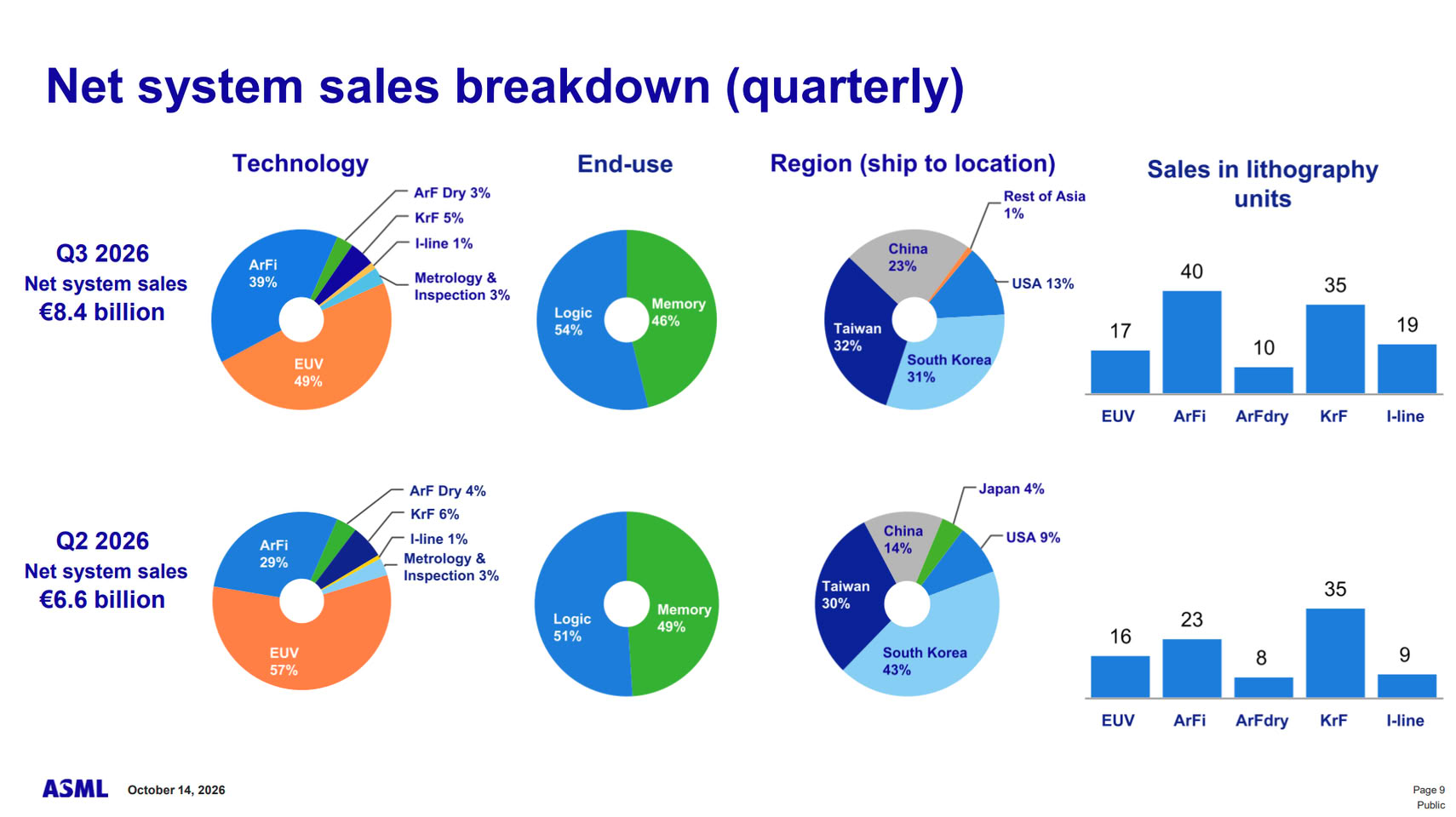
ASML today reported its Q3 2026 financial results, with gross revenue totaling €11.7 billion, a gross margin of 57.5%, and a net income of €5.0 billion. ASML also provided updates on its system sales by region, revealing that shipments to China have become one of its strongest areas for system sales. Chinese semiconductor manufacturers are rushing to stockpile more tools. In the previous Q2, net system sales to China accounted for 14% of ASML's sales. In the latest Q3, this figure has grown to 23%, nearly a quarter of all ASML's system sales. In Q3, Taiwan remains the largest buyer of ASML equipment at 32%, followed by South Korea at 31%. China takes third place with 23%, and the United States follows with 13%.

The strong demand from China is reportedly due to Chinese memory and storage makers stockpiling enough lithography tools from ASML to support their expansion plans for the next three years, even if they are cut off from the supply chain. According to earlier reports, memory maker CXMT and storage giant YMTC have secured sufficient DUV lithography tools from ASML to support their growth plans for the next three years, despite increasing tensions and potential bans on exporting these older DUV tools to China. The United States government is reportedly pressuring the Dutch government to completely halt tool exports to China.

Intel "Panther Lake" Reportedly Gets Up to 20% Price Hike, Older Generations Also Impacted

Intel is reportedly preparing for a significant price increase across its silicon designs, according to supply chain sources cited by Commercial Times Taiwan. The first to experience this price hike is the latest "Panther Lake" processor generation, built on the Intel 18A node, with an increase ranging from 15% to 20% depending on the SKU. Intel reportedly made these adjustments on September 1, but consumer price increases have not yet been observed, or it may take a few more weeks for the old supply to clear. This supply-side price hike doesn't mean that Intel is directly changing its consumer pricing, but rather adjusting the pricing for major laptop OEMs such as Acer, ASUS, Lenovo, Dell, and HP. With a potential 20% price hike, this could translate to a few dozen US dollars more for the OEMs. Laptop manufacturers are likely to pass these increased costs onto consumers, especially given the current challenges with memory and storage pricing, which are already squeezing margins.

The reported price hikes don't stop there. The "Meteor Lake" and "Arrow Lake" processor families are also expected to see price increases, with reports indicating a 5% to 10% hike for these two generations, depending on the SKU. Intel sources silicon from both TSMC and its internal foundry, but the demand for silicon in the form of CPUs is skyrocketing in the age of AI, making price increases likely. Consumer demand remains, but much of the available CPU manufacturing capacity, both internally and externally, is being absorbed by agentic AI workloads, which are pushing server configurations to a 50:50 ratio of CPUs to GPUs.

AMD CEO Lisa Su Says 2027 Will Bring a "Substantial" Supply Increase

AMD will "substantially" increase its chip supply in 2027, CEO Lisa Su told reporters in Taipei on Tuesday, while admitting that demand is still running ahead of what the company can ship. Su is on her third trip to Taiwan this year, meeting partners such as Foxconn, Quanta, Acer, and ASUS, with TSMC also on the schedule. She is reportedly heading to South Korea later this week to sit down with memory suppliers Samsung and SK Hynix. Here's what she said:
We've been able to increase our supply as we've gone through 2026, and we're going to substantially increase our supply in 2027, but we can definitely use more. There's very, very high demand for the next several years. We can see very high demand, and so we need more advanced wafer capacity.

TSMC Reportedly Evaluating Texas Expansion Besides $265 Billion Arizona Plan

Taiwan's Economic Daily News (UDN) reports that TSMC is planning a second US manufacturing campus in Texas, separate from Arizona. Citing semiconductor equipment industry sources, it says the project would include six advanced fabs, with Dallas the most likely location. UDN estimates the total investment could exceed the $265 billion committed to Arizona, since new fabs would probably use more advanced nodes. TSMC hadn't commented when the report went out. Reuters has since reported, citing two people familiar with the matter, that TSMC is indeed evaluating a potential Texas investment, with plans not finalized. One source said it would come on top of the Arizona commitment.

UDN points to customers like NVIDIA, Intel, AMD, and Apple wanting US-made chips, plus the Trump administration's renewed tariff threat of up to 200% for chipmakers that don't produce in the US. TSMC reportedly hasn't asked suppliers to prepare, and the board hasn't signed off just yet. TSMC added another $100 billion to its Arizona plans in July, but UDN says that site still faces power and labor shortages while it sorts out its water supply. Either way, fabs like these take years to build, so it's not reasonable to expect Texas-made chips any time soon.

Intel Z990 Motherboards Spotted In Shipping Records Ahead Of Nova Lake Launch

Some Z990 motherboards for Intel's upcoming Nova Lake platform have started showing up in shipping records, suggesting the launch is getting closer. Club386 spotted at least five boards with "Z990" in their names listed in customs data from Taiwan and Vietnam, dated July 2026.

Z990 is expected to be the flagship chipset for Nova Lake-S, Intel's next Core Ultra desktop lineup on the new LGA1954 socket. Intel is also prepping a cheaper Z970 chipset that keeps multiplier overclocking but offers a less diverse expansion suite overall. Also, these aren't the first Z990 boards spotted in the wild either. A Gigabyte AORUS Z990 Pro turned up at Computex earlier this year with its socket taped over, though the branding gave it away. With boards already moving through shipping channels, Nova Lake's early 2027 window looks increasingly realistic, though the rumored 52-core flagship apparently won't arrive until later in the year.

AMD Plans 10% Price Hike Across GPUs, Chipsets, and Possibly CPUs

AMD is preparing for a series of price hikes in response to rising costs of acquiring silicon from its supply chain. According to ChannelGate, AMD is working on a 10% price increase across its products due to the upstream supply chain squeeze. Since most of AMD's silicon is manufactured by Taiwanese semiconductor giant TSMC, any change in wafer pricing forces AMD to pass these costs onto customers. Reportedly, TSMC is increasing the pricing of its silicon wafers, and as a result, AMD must raise its product costs to maintain margins and keep the business afloat. The price increases will affect almost every product AMD offers, including GPUs, possibly CPUs, and even motherboard chipsets.

For CPUs and GPUs, AMD has already implemented price hikes in the past, driven by a combination of demand and high DRAM pricing. However, this is one of the first instances where AMD is increasing the pricing of its motherboard chipsets, which will require motherboard makers to adjust their pricing accordingly. If TSMC implements a 10% price hike across its nodes, from 2 nm N2 to some older mature nodes, AMD will have to pass these costs onto partners and consumers, who will ultimately bear the difference. As a fabless chip designer, AMD cannot dictate or negotiate for lower rates for wafers from TSMC.

Transcend Launches 64 GB DDR5-6400 CUDIMM and CSODIMM Embedded DRAM Modules

Transcend Information, Inc. (Transcend), a leading global manufacturer of memory and storage solutions, has introduced its DDR5-6400 CUDIMM and CSODIMM embedded DRAM modules, offering capacities of up to 64 GB per module to meet the computing demands of edge AI, smart manufacturing, industrial automation, and high-performance embedded systems. Featuring DDR5's dual-channel architecture and a low operating voltage of 1.1 V, the modules incorporate a Client Clock Driver (CKD) to minimize signal interference caused by noise and jitter during high-speed operation, thereby enhancing signal stability. An integrated power management IC (PMIC) further improves power efficiency and voltage regulation. The SPD chip features a built-in temperature sensor for real-time memory temperature monitoring, while a transient voltage suppressor (TVS) helps protect components from damage caused by voltage fluctuations. In addition, On-Die ECC built into the DDR5 DRAM chips enhances data integrity and long-term operational reliability. Together, these features provide next-generation industrial computing platforms with a high-capacity, high-performance, and dependable memory solution.

Up to 64 GB per Module for Demanding Industrial Applications
Transcend's DDR5-6400 CUDIMM and CSODIMM modules offer capacities of up to 64 GB per module, meeting the intensive computing requirements of industrial computers, edge computing devices, and embedded systems. DDR5's dual-channel architecture improves data access efficiency and overall transfer performance, while DDR5-6400 speeds accelerate large-scale data exchanges and real-time processing. The modules provide the capacity and bandwidth required for high-performance industrial applications.

TSMC and ASML Announce Initiative to Pioneer Industry Transition to Large-Format Photomasks for High NA EUV

ASML Holding N.V. (Euronext: ASML, Nasdaq: ASML) and Taiwan Semiconductor Manufacturing Company (TWSE: 2330, NYSE: TSM) announced a collaborative initiative to lead the semiconductor industry's transition to a larger-format Extreme Ultraviolet (EUV) lithography photomask.

While High NA EUV will be adopted for production using the current, 6-inch masks, the transition to larger, 12-inch masks is expected to further increase fab productivity, lower chipmaking costs and remove stitching constraints, benefiting the entire semiconductor industry. It will enable advanced chip manufacturers to fully leverage the advantages of High NA EUV, making future generations of leading-edge chips more cost-effective.

Taiwanese Hardware Manufacturers Sell Out NVIDIA RTX Spark Laptop Stock Ahead of Launch

News out of Taiwan suggests that both ASUS and MSI have sold their entire production run of NVIDIA RTX Spark based laptops before a single unit has shipped. It would appear that allocation of the MediaTek co-developed chip has been pretty sparse by NVIDIA, which is one reason for the first stock being sold out. Investor.com.tw claims that ASUS and MSI were allocated 100,000 units of the N1 and/or N1x version of the SoC for their first production run, which doesn't seem like a super-small amount, although it's unclear how many chips NVIDIA's other launch partners were allocated.

Dell, HP, Lenovo and Microsoft are the other RTX Spark launch partners, with Acer and Gigabyte said to be following later. According to the source above, NVIDIA will be providing a higher allocation for the next production run, of somewhere between 300 and 500,000 chips. Considering that there's an expected starting MSRP of somewhere around US$3,500 for an RTX Spark laptop in Taiwan, it doesn't seem like there might be as much demand for these new laptops as the channel might think, unless they know something that isn't public information as yet. Nonetheless, it'll be interesting to see how well received NVIDIA and MediaTek's Arm based laptop SoC will be and if the asking price will be a hurdle or not.

Samsung New Memory Roadmap: HBM5 Aims for 2x Performance, zHBM for 8x

Samsung presented its updated memory roadmap at SEMICON Taiwan 2026, with HBM5 and the upcoming zHBM architecture being the main focus points while setting ambitious goals and expectations. According to Samsung, HBM5 is targeting twice the performance and 20% higher performance per watt compared to HBM4E, alongside a 20% reduction in thermal resistance. As changes, the base die moves from the 4 nm process used in HBM4 and HBM4E to Samsung's in-house 2 nm node, and the stack options expand to 12, 16, and 20 layers. Mass production is expected around 2028. Recently, Samsung confirmed at the Hot Chips 2026 conference's Advance Program that the company is preparing to ship HBM4E memory with speeds of 16 Gbps per pin. Samsung is currently shipping HBM4 that works at 11.7 Gbps per pin.

zHBM uses a more radical approach, rather than placing memory beside the accelerator as conventional HBM does, zHBM stacks memory directly on top of the processor, shortening the data path and delivering higher bandwidth and efficiency. With zHBM, Samsung is targeting eight times the raw performance and three times the performance per watt of HBM4E, with thermal resistance reduced by 75-90%. At FMS 2026, Samsung unveiled the industry's first concept models of zHBM and is expected to launch this completely different architecture after 2029. Rethinking the HBM architecture appears to be the direction the industry is heading. NVIDIA recently announced its own NVHBM custom memory that moves the memory controller into the HBM base die rather than keeping it on the compute die.

Micron Unveils U.S.-Based Research Labs to Shape the Future of Memory and AI

Micron Technology, Inc. (Nasdaq: MU) today unveiled Micron Research Labs, a U.S.-based long-horizon premier research institution headquartered in Boise and backed by a planned $10 billion investment over the next decade. Building on Micron's technology and manufacturing leadership, the new hub will bring together customers, academia, government and the broader semiconductor ecosystem to pursue breakthroughs beyond today's technology roadmaps and help define what's possible in the decades ahead. Key research areas include critical memory technologies, advanced memory and compute architectures, packaging and future semiconductor manufacturing.

As the first dedicated memory research hub of its kind in the U.S., Micron Research Labs will center on a flagship Boise campus designed to support advanced research across critical technology domains. The planned investment will also fund extensive university collaborations, global satellite labs and deep ecosystem partnerships, creating a connected research network focused beyond the next generation of technologies for the AI era.

Samsung Foundry Prepares Price Hikes After Massive Demand Spike

According to Reuters, Samsung Foundry is experiencing a significant increase in customer orders, prompting the company to adjust its pricing strategy across multiple nodes. In July, Samsung raised the price of its 4 nm node, known as SF4, by about 10-15% for customers in the United States and China, while customers in Taiwan saw a more modest increase of 5-10%. Prices for wafers produced with the 5 nm node, referred to as SF5, also rose by 10-15%. Interestingly, even the older 8 nm node experienced a 10% price hike. This increase for the SF8 node is likely due to NVIDIA placing orders for its GeForce RTX 3060, a product the company has reintroduced after several generations.

There is no mention of price hikes for newer nodes such as Samsung SF2, SF3, and their variations. It seems Samsung anticipated the level of external customer demand for these nodes, and they are already quite costly. Notably, Reuters reports that U.S.-based customers are prioritized after Samsung's internal chip demand for its own SoCs, while China-based design houses are third in line. However, as China seeks advanced nodes, they are willing to accept higher price increases to secure allocation at Samsung Foundry at any cost.

HBM Shipments to Malaysia Surge, Pointing to Intel's "Project Pelican" Facility

According to SemiAnalysis Chipbook data on exports from South Korea, a significant portion of high-bandwidth memory exports is now heading to Malaysia, reducing shipments to Taiwan. This indicates that the HBM memory used by TSMC for its CoWoS family of advanced packaging technologies—CoWoS-S, CoWoS-L, and CoWoS-R—are increasingly being replaced an unknown packaging facility in Malaysia. Presumably, the only fab capable of integrating so much HBM into product is Intel, known for its advanced packaging technology like EMIB and Foveros. Since TSMC operates no advanced packaging facility in Malaysia, and other players in that country being very small for now, the only logical option is Intel.

Late last year, Intel entered the final phase of its "Project Pelican," an advanced packaging complex in Malaysia, completing the $7 billion buildout. This facility is equipped for die sort and die prep operations and will support both EMIB and Foveros packaging flows, allowing Intel to respond more quickly to customer needs. With Intel's EMIB and Foveros being among the world's most advanced packaging technologies, the large influx of HBM into Malaysia suggests that Intel's foundry customers for advanced packaging services are increasing, diverting demand from TSMC. The data shows that about $1.3 billion worth of HBM is now going to Malaysia, while less than $3 billion is going to Taiwan. This is a significant decrease from over $5 billion going to Taiwan just a few months ago.

TSMC Achieves 98% Yield on CoWoS-L with 5.5x Reticle Size, 14x Comes in 2029

TSMC has reportedly achieved near-perfect packaging yields, establishing a baseline of about 98% for its current CoWoS advanced packaging. This technology accommodates a die area equivalent to 5.5 times the reticle limit, or about 858 mm². As a result, packaging 4,720 mm² worth of silicon on CoWoS-L is now possible, with only 1-2% of the packaged designs experiencing issues. This is a significant achievement for a packaging technology that went into mass production earlier this year. Although CoWoS-L has been shipping for some time, this year marks the first time a 5.5x reticle chip has been packaged on a mass production scale.

The Taiwanese manufacturing giant is also preparing for even larger designs, including up to 14x reticle size dies on a single, enormous package. This means a silicon area of 12,012 mm² will be packaged using TSMC's CoWoS, or specifically one of its variants. This technology is slated for 2029, when its A13 node is expected to be in mass production. TSMC's timelines are consistently being met with customer satisfaction, and the company continues to sell out its manufacturing and advanced packaging technologies. However, creating any design beyond the 3x reticle limit must be done carefully, as thermal warping can introduce mechanical issues. The company is constantly working with customers to overcome these challenges.

CXMT Surpasses 90% DDR5 Yield, Challenges Industry Giants

Chinese memory giant CXMT has reportedly achieved a significant milestone in DDR5 production, with manufacturing yields now comfortably above 90%. This is comparable to what major manufacturers like Samsung, SK hynix, and Micron are achieving. According to reports, CXMT uses a 17 nm node for DDR5 chip production and has reached a 90% yield for these chips. This is only 2-3% lower than Samsung's yield on its 10 nm class node for DDR5 production, indicating that CXMT's production quality is matching that of the world's largest memory maker. This is a remarkable achievement for a company that excels in cleanroom construction time, taking only 12 months to build its fab's cleanroom compared to the two years others require. As the company plans to end the year with 350,000 DRAM wafers per month, high yields mean there is little waste or leftover.

Chinese MyDrivers also notes that PC OEMs have mixed reactions to adopting CXMT DRAM in their products. For instance, Dell has completely banned the use of CXMT in its machines, while HP only allows CXMT DRAM in its Chinese PCs. Major Taiwanese brands such as ASUS and Acer have increased adoption in some models, as they have more flexibility in supply chain procurement. However, both companies use CXMT memory for PCs sold in mainland China and some emerging markets, meaning the West is still far from receiving PCs with CXMT memory modules. PC OEMs are also cautious about procuring CXMT memory due to concerns about disrupting their relationships with the big three memory makers.

Sony Semiconductor Solutions and TSMC Establish Joint Venture for Next-Gen Image Sensors

Sony Semiconductor Solutions Corporation ("Sony") and Taiwan Semiconductor Manufacturing Company Limited ("TSMC") (TWSE: 2330, NYSE: TSM) today announced the execution of a legally binding definitive agreement for the establishment of Advanced Vision Semiconductor Manufacturing Corporation as a joint venture ("JV") in Koshi City, Kumamoto Prefecture, Japan. The JV will serve as a core hub for the development and manufacturing activities required for the volume production of image sensors for smartphones utilizing advanced manufacturing process technology. The JV is expected to commence volume production in 2029.

Sony will be the sole controlling shareholder and the JV is planned to operate as a consolidated subsidiary of Sony Group Corporation. The Representative Director of the JV is planned to be appointed by Sony.

Nanya Announces $10.7B Investment in Fab5A, Aims for 10 nm-Class EUV DRAM

Nanya Technology Board of Directors announced on August 5 that the company has launched its largest investment program, committing up to NT$346.6 billion (around $10.7 billion) to its Fab5A facility through 2026-2029. The project covers 10 nm-class processes from 1b through 1e nodes and introduces EUV lithography. Nanya has also increased its 2026 capital expenditures budget by 34% to NT$69.7 billion (around $2.16 billion). The extra NT$17.7 billion is going toward advance payments for equipment to keep Fab5A on schedule. The production roadmap has wafer starts being produced in the second half of 2027, reaching 30,000 wafers per month in 2028 and 35,900 in 2029. The maximum planned capacity is around 45,000 wafers monthly. The 1c pilot production has already begun, while the 1d node is under development and expected to enter pilot production soon. Nanya Fab5A investment, when completed, is estimated at roughly $16 billion, deployed in phases based on market demand.

Commercially, Nanya is having a strong run. July revenue hit NT$43.87 billion (around $1.3 billion), up 49.3% month over month and 719.6% year over year, driven by continued DRAM price increases, particularly sharp gains in DDR4 contract prices. Remember that just a year ago DDR4 module prices overtook DDR5 for the first time, with Nanya among the biggest beneficiaries. Its customers include giants like NVIDIA, Google, Microsoft, Intel, AMD, and Qualcomm, with the future looking great for the Taiwanese company. Its long-term agreements reportedly now cover about 50% of production capacity, with short-term contracts gradually converted into long-term agreements.

TSMC Develops EMIB-like Technology to Compete with Intel

TSMC is reportedly developing an advanced packaging technology to rival Intel's Embedded Multi-die Interconnect Bridge (EMIB), which the company internally refers to as EMIB-like. According to sources close to The Information, TSMC's Chip-on-Wafer-on-Substrate (CoWoS) packaging might lose some customers to Intel's EMIB. As a result, TSMC has begun developing its EMIB-like technology. This development will reportedly be supported by Taiwan's Kinsus Interconnect Technology, which will assist TSMC in developing, scaling, and manufacturing the CoWoS alternative without issues. TSMC currently offers three versions of CoWoS: CoWoS-S, CoWoS-L, and CoWoS-R.

CoWoS-S is the first generation of CoWoS, utilizing a full monolithic silicon interposer with TSVs for maximum routing density and performance. Then, there is CoWoS-L that takes a hybrid approach, replacing the full silicon sheet with a more affordable organic base and embedding small localized silicon bridges (LSI) only where high-speed die-to-die communication occurs. This allows for large layouts to bypass reticle limits through bridge stitching. CoWoS-R is the third option that completely replaces silicon with an organic copper/polymer RDL interposer. It experiences a slight reduction in signal attenuation and routing density, but its mechanical flexibility makes it highly scalable and cost-effective for large-die chips.
Return to Keyword Browsing
Nov 11th, 2026 03:13 CST change timezone

New Forum Posts

Popular Reviews

TPU on YouTube

Controversial News Posts