Friday, August 14th 2020

NVIDIA GeForce RTX 3090 "Ampere" Alleged PCB Picture Surfaces

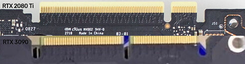
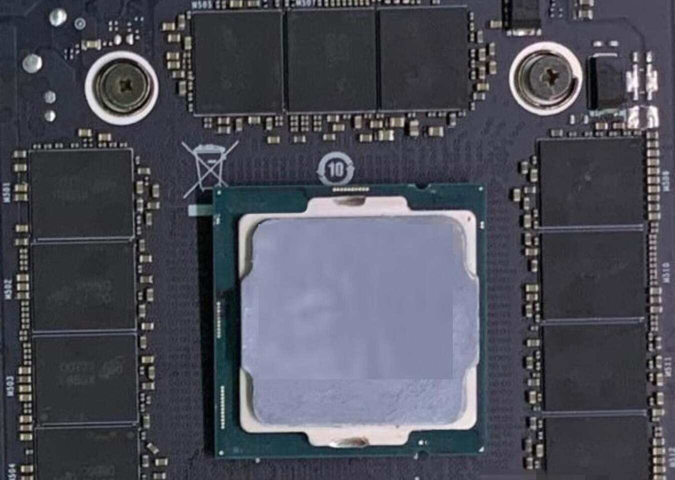
As we are getting close to September 1st, the day NVIDIA launches its upcoming GeForce RTX graphics cards based on Ampere architecture, we are getting even more leaks. Today, an alleged PCB of the NVIDIA's upcoming GeForce RTX 3090 has been pictured and posted on social media. The PCB appears to be a 3rd party design coming from one of NVIDIA's add-in board (AIB) partners - Colorful. The picture is blurred out on the most of the PCB and has Intel CPU covering the GPU die area to hide the information. There are 11 GDDR6X memory modules covering the surrounding of the GPU and being very near it. Another notable difference is the NVLink finger change, as there seems to be the new design present. Check out the screenshot of the Reddit thread and PCB pictures below:
NVIDIA GeForce RTX 3090 PCB NVIDIA GeForce RTX 3090 PCB NVIDIA GeForce RTX 3090 PCB
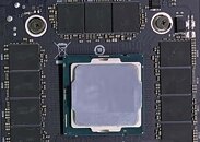
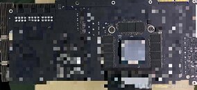
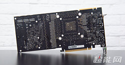
More pictures follow:

NVIDIA GeForce RTX 3090 PCB
Source: VideoCardz
Add your own comment

72 Comments on NVIDIA GeForce RTX 3090 "Ampere" Alleged PCB Picture Surfaces
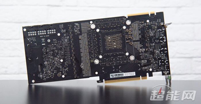
#27
beautyless
Can it handle 4k at 120fps with all settings maxed out?
Posted on Reply
#28
ZoneDymo
beautylessCan it handle 4k at 120fps with all settings maxed out?
Depends on the game?
Posted on Reply
#29
moproblems99
It will be interesting to see how much power draw and heat matters this generation. I can sense a little walk back about how important they are...
Posted on Reply
#30
iO
Wow that card will cost a fortune.

And how do you cool that memory with its ~40 Watts thermal output without making the card a 4 slot monster because of a giant backplate...
Posted on Reply
#31
medi01
beautylessCan it handle 4k at 120fps with all settings maxed out?
Yes, if 2080Ti can handle that game at 4k and 90fps.
Posted on Reply
#32
ThrashZone
Crackong3 x 8-pin .........

Quite an electric heater
Hi,
Might just mean it needs it's own source of power instead of sharing making the current more stable.
Posted on Reply
#33
Th3pwn3r
Shatun_BearWith 3X 8-PIN power connectors, this is a 500W+ card. Something wrong has happened with Ampere that they need to draw that much power to offer a generational leap over the 250-300W 2080 Ti. Yes, rumours are this is 40% faster than that card, but it draws about 40% more power. So the rumours of Nvidia going with the borked Samsung 8nm process instead of TSMC's superior 7nm+ appear true.
You're assuming maximum draw. It might have the ability to support that draw but might not have to.
Posted on Reply
#34
RedelZaVedno
There are leaks saying that 3090 (or whatever it is called) will target 350W peak power draw (PPD), BUT NVidia will allow user to remove power limiter, so that one can increase boost clock speeds past 2Ghz resulting in 400-500W PPD. It makes perfect sense if Ampere is on Samsung's 8nm node (comparable to 10nm TSMC's density). RDNA2 will boost at least to 2.23 GHz (confirmed by Sony's SP5 specs) on 7nm node so Ampere on 8nm will need A LOT of power draw to match it's frequency. I have no doubt Ampere's architecture would be much more power efficient than RDNA2's IF on 7nm, but Samsung's 8 nm is a big problem for Nvidia. We will likely see top tier Ampere GPUs migrating to 7 nm as soon as TSMC gives NVidia needed production capacities (probably in 2021 or 2022 when AMD Zen CPUs move to 5 nm).
Posted on Reply
#35
mouacyk
May be NVidia figured out that to get rid of RT performance penalty, they need to throw another 150W at the problem. Or, it's a custom design. I am glad for a full 384-bit memory SKU again, unlike the compromised 320-bit and 352-bit ones we had been handed.
Posted on Reply
#36
berjerac
Memory on the backside is probably the reason why FE has coolers on both sides.
Posted on Reply
#37
jabbadap
Vya DomusWell, you can also see that it has three 8-pin connectors. On a reference card ...
To me it's look like a pic of custom RTX2080ti. That nvlink finger is from Turing, not from Ampere. And that blurred image is just that, blurred.
Posted on Reply
#38
Wshlist
3 x 8 pin, hmm, maybe it's the new 'macro transistor' technology intel is rumored to have developed :P
Posted on Reply
#39
Assimilator
Am I the only one who's noticed that www.techpowerup.com/img/6Rv0dLid3gLg9qpO.jpg is a completely different PCB to the one shown in the first two images?

The first two have only 11 memory chips and the alleged Ampere NVLink fingers, the third has pads for 12 chips and the Turing NVLink fingers.
steen384bit. One module between GPU die & PCIEx16 connector...
Where?
Posted on Reply
#41
Assimilator
steenRight where I said. Squint... ;)
Everything except the 11 chips is blurred out.
Posted on Reply
#42
steen
AssimilatorEverything except the 11 chips is blurred out.
Heh, still not convinced? 1st pic, bottom right GDDR6X module. PCB component label is...?
Posted on Reply
#43
berjerac
Does anybody know if Ampere FE will have usb-c port? No mentions so far.
Posted on Reply
#45
jabbadap
Petey8080What im wondering is why is the gpu die on the back side of the card
Well maybe it's a dual gpu card. Could explain the name RTX 3090 too...
Posted on Reply
#46
my_name_is_earl
Obviously leak by Nvidia themselves. Real leak doesn't have blur boxes on them. Marketing BS.
Posted on Reply
#47
Fluffmeister
moproblems99It will be interesting to see how much power draw and heat matters this generation. I can sense a little walk back about how important they are...
Well hey, Vega 64 sold, offering GTX 1080 levels of performance despite being horrendously late and super juicy compared to the competition. I guess that's when undervolting became a hobby too.
Posted on Reply
#48
JAVAD
beautylessCan it handle 4k at 120fps with all settings maxed out?
It depends on the type of game. Of course, the type of graphics engine and game genre are also influential.
Posted on Reply
#49
ARF
nVidia hasn't had a *9* card since the dual-GPU GTX 690.
Posted on Reply
#50
Valantar
For those of you claiming there's a 12th memory die below the gpu die area: that darker section is an artifact of the blur used to mask the board. Look closely and it's clear that that area does not comprise of a die like the others, but three dark blurred blocks. I would guess they stem from blurring an area shaded by the CPU placed there. Besides, putting a die there would make its traces either much shorter (directly to the die) or longer (around a corner of the die) than the rest of the memory, which would essentially break it. Memory timings are far too tight to allow for unequal trace lengths. This board fits 11 memory chips on each side.
TheDeeGeeMy GTX 680 4GB had them on the back as well.
That sure qualifies as "it's been a while", no?
steen384bit. One module between GPU die & PCIEx16 connector...
No. See above. And it definitely won't be 22GB on a 384-bit bus...


For those of you saying that the CPU for some reason covering the area behind the die somehow confirms the RT coprocessor hypothesis: no. Not only would a chip there make providing stable power to a GPU die on this level near impossible due to forcing crucial power conditioning components further from the die, but the mounting of such a chip would make the PCB ridiculously expensive (dense and high bandwidth vias through the PCB, while not blocking or otherwise interfering with everything else going there?), and if such a coprocessor had any power draw at all it would be impossible to cool in a standard PCIe form factor - you'd need a full slot of heatsink at the back as well. 4-slot card that fouls your CPU cooler, anyone? Yeah, not happening. And besides, the added latency from moving RT processing off-die - even using exotic interconnects - would make it impossible to implement at anything resembling high frame rates and good frame times.

Im guessing the CPU is either there to hide identifying information as to the source (company), or to mess with people who believe in this rumor.
Posted on Reply
Add your own comment
Apr 19th, 2024 12:17 EDT change timezone

New Forum Posts

Popular Reviews

Controversial News Posts