Friday, November 27th 2020

TSMC Completes Its Latest 3 nm Factory, Mass Production in 2022

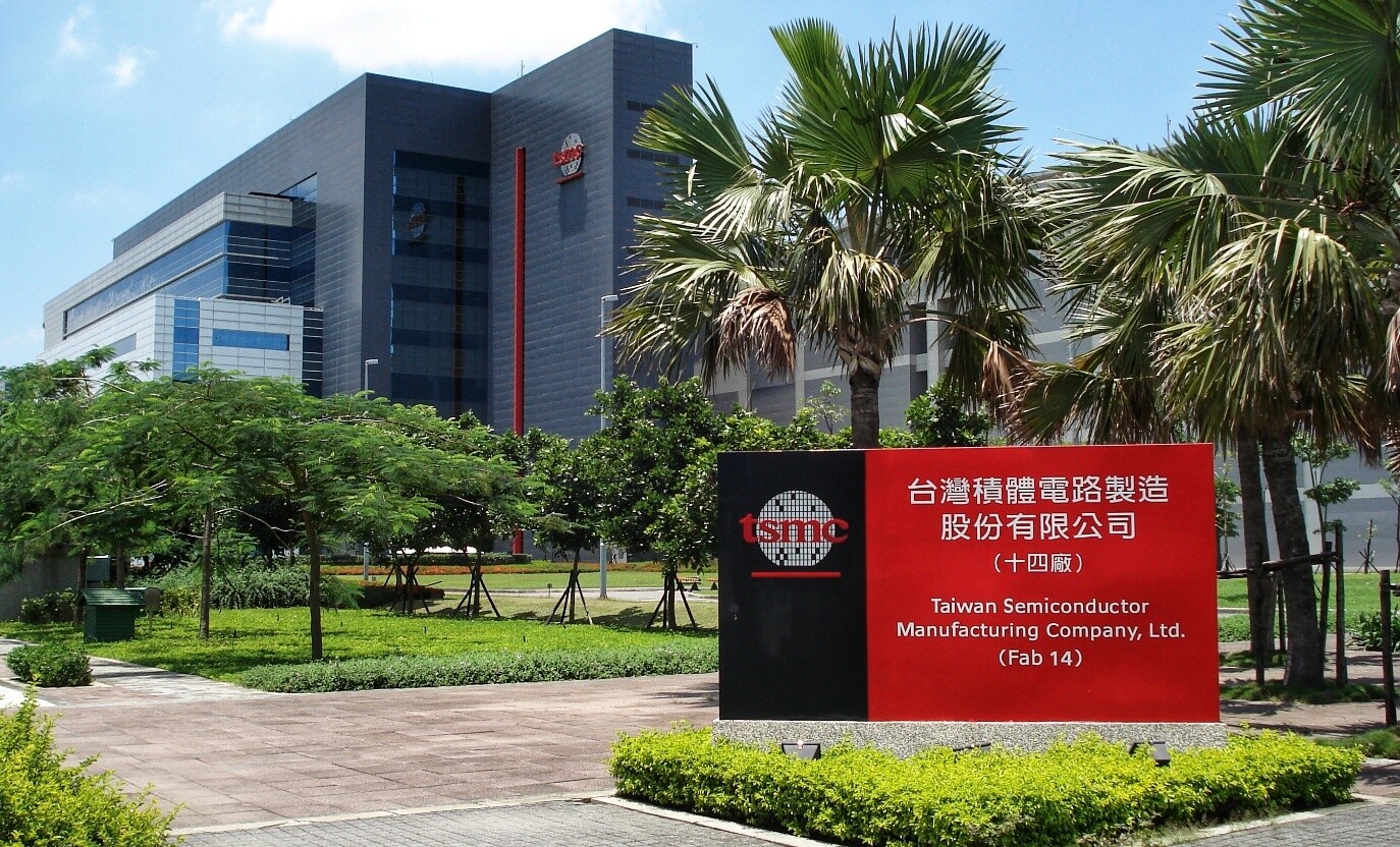
They say that it is hard to keep up with Moore's Law, however, for the folks over at Taiwan Semiconductor Manufacturing Company (TSMC), that doesn't seem to represent any kind of a problem. Today, to confirm that TSMC is one of the last warriors for the life of Moore's Law, we have information that the company has completed building its manufacturing facility for the next-generation 3 nm semiconductor node. Located in Southern Taiwan Science Park near Tainan, TSMC is expecting to start high-volume manufacturing of the 3 nm node in that Fab in the second half of 2022. As always, one of the first customers expected is Apple.

Estimated to cost an amazing 19.5 billion US Dollars, the Fab is expected to have an output of 55,000 300 mm (12-inch) wafers per month. Given that the regular facilities of TSMC exceed the capacity of over 100K wafers per month, this new facility is expected to increase the capacity over time and possibly reach the 100K level. The new 3 nm node is going to use the FinFET technology and will deliver a 15% performance gain over the previous 5 nm node, with 30% decreased power use and up to 70% density increase. Of course, all of those factors will depend on a specific design.
Source: Tom's Hardware
Add your own comment

56 Comments on TSMC Completes Its Latest 3 nm Factory, Mass Production in 2022

#1
Vya Domus
As always, one of the first customers expected is Apple.
Are they ? I thought they were supposedly switching to Samsung, things didn't quite turn out the way the wanted to, huh ?
Posted on Reply
#2
Space Lynx
Astronaut
If they can build a 3nm fab and it's already done, why build a 5nm one Arizona where construction just started... I don't care who the customer is, it doesn't make sense... lol
Posted on Reply
#3
AleksandarK
News Editor
Vya DomusAre they ? I thought they were supposedly switching to Samsung, things didn't quite turn out the way the wanted to, huh ?
Apple might expand to Samsung as well, but TSMC is its primary manufacturer.
lynx29If they can build a 3nm fab and it's already done, why build a 5nm one Arizona where construction just started... I don't care who the customer is, it doesn't make sense... lol
It is TSMC's entry to US soils, the 5 nm node is already in production in Taiwan, where Apple gets its M1 chips from. It is just a Fab on US soils.
Posted on Reply
#4
Space Lynx
Astronaut
AleksandarKApple might expand to Samsung as well, but TSMC is its primary manufacturer.


It is TSMC's entry to US soils, the 5 nm node is already in production in Taiwan, where Apple gets its M1 chips from. It is just a Fab on US soils.
I still don't get it. If you are a for-profit business, then you go balls to the walls as soon as your engineers give you the thumbs up, and you rake in the $$$$$ If 3nm is greenlit, and it apparently is, then you go full pedal to the medal on it on a new construction project. The world doesn't have enough natural resources left to keep playing milking games.
Posted on Reply
#5
AleksandarK
News Editor
lynx29I still don't get it. If you are a for-profit business, then you go balls to the walls as soon as your engineers give you the thumbs up, and you rake in the $$$$$ If 3nm is greenlit, and it apparently is, then you go full pedal to the medal on it on a new construction project. The world doesn't have enough natural resources left to keep playing milking games.
The Arizona fab is built so it can be close to US and maybe used by the government, it doesn’t matter what is the technology, but rather the political impact TSMC.
Posted on Reply
#7
Vya Domus
medi01@Vya Domus ,

could you help me estimate number of RDNA2/Zen3 chips per wafer?
Asking fecause:

Hard to tell exactly but with the rumored defect density and size per chip it must be around 60 Navi21 good chips per wafer +/- 5 out of 96 but the number of useful dies is higher because some can be reused. Anyway I speculated a long time ago there wont be many RDNA2 chips out there because of this reason (consoles and servers).

As far as NVIDIA goes, it could be as low as 35 GA102 dies per wafer out of 79, but those are fully functional and NVIDIA currently only has Quadros using the fully enabled die. My guess is that the yields are probably even worse.
Posted on Reply
#8
Sovsefanden
So this means Apple SoCs will be 3nm in 2022
Posted on Reply
#9
ratirt
lynx29I still don't get it. If you are a for-profit business, then you go balls to the walls as soon as your engineers give you the thumbs up, and you rake in the $$$$$ If 3nm is greenlit, and it apparently is, then you go full pedal to the medal on it on a new construction project. The world doesn't have enough natural resources left to keep playing milking games.
You can go 3nm when you get customers and you give them reasonable price. Apparently the price for the 3nm node is not that cheap as of now besides there is still huge demand for the 7nm node. Why force 3nm when you still get piles of money from 7nm?
Posted on Reply
#10
londiste
medi01could you help me estimate number of RDNA2/Zen3 chips per wafer?
Zen3: 83.736 mm² (11.270 x 7.430 mm) (link)
Navi21: 519.8 mm² (28.49 x 18.25 mm)

Die Yield Calculator: caly-technologies.com/die-yield-calculator/
Wafer Diameter for 7nm should be 300mm.
Defect Density was 0.09 last time it leaked, it may have improved but not by much.

Zen3: 694 dies total, 644 good dies (with defect density 0.09)
Navi21: 107 dies total, 68 good dies (with defect density 0.09)

In addition to Zen3 and Navi21, there is the die MI100 is based on that is definitely not small or easy to produce (but I bet is very profitable).

TSMC 7nm capacity is 130K wafers/month, planned to increase to 140K wafers/month by end of 2020.
Based on various news/leak/rumor bits AMD at this point has about 60-65% of that capacity, lets say roughly 80K wafers/month.

- From Sony's planned at least 7 million PS5s manufactured in this year and knowing the rough size of the PS5 APU, they need at least 15K wafers/month to get these manufactured. This is probably an optimistic number, assuming perfect yields (leaks/rumors say are yields are not quite good), 20-25 K wafers/month sounds realistic.
- Xbox is probably in the same range. Microsoft has not been public about the amount manufactured but I bet it will not be much less. Xbox APU is bigger, so less per wafer and probably slightly worse yields. That's another 20-25K wafers/month.
- Since neither Sony nor Microsoft are listed as big TSMC customers, that must be coming out of AMD's 7nm allocation. Basically - half or more of AMD's TSMC 7nm allocation goes to manufacturing console APUs at this point. Numbers are assuming equal manufactured amounts of APUs over 2020-H2.

Edit:
Aaaand... I do read the referenced news bit but do not register any of it somehow.
Wafer amounts in the news:
- 150K/quarter is 50k/month. Less than I expected.
- 120K/quarter - 40k/month. Close enough to what I expected but there are about half as much Xbox APUs produced than PS5.
Posted on Reply
#11
Sovsefanden
AleksandarKApple might expand to Samsung as well, but TSMC is its primary manufacturer.


It is TSMC's entry to US soils, the 5 nm node is already in production in Taiwan, where Apple gets its M1 chips from. It is just a Fab on US soils.
Apple is TSMC's highest priority and best customer

Apple gets exclusity on all new nodes, for months and months before anyone else can get in
Posted on Reply
#12
Frick
Fishfaced Nincompoop
lynx29If they can build a 3nm fab and it's already done, why build a 5nm one Arizona where construction just started... I don't care who the customer is, it doesn't make sense... lol
Not everything has to be bleeding edge. There's many, many, many things that does fine on even >20nm.
Posted on Reply
#13
Sovsefanden
lynx29If they can build a 3nm fab and it's already done, why build a 5nm one Arizona where construction just started... I don't care who the customer is, it doesn't make sense... lol
More advanced = more expensive (both the facility and the end-chips)
Posted on Reply
#14
HTC
The new 3 nm node is going to use the FinFET technology and will deliver a 15% performance gain over the previous 5 nm node, with 30% decreased power use and up to 70% density increase. Of course, all of those factors will depend on a specific design.
As we know, since the introduction of 7nm we've been having hot spots where heat concentrates to high degree: a perfect example being the 5800X, which is much hotter than the 5950X (though the base clock of 5950X being lower is a variable to be considered), even though the 5950X is essentially twice the 5800X (minus one extra IO die, ofc). This happens because the heat is spread to a wider area so the cooler does it's job better on the 5950X VS the 5800X.

But if we increase the density further? How does that affect cooling capability? And it's up to 70% increase OVER 5NM, not 7nm, which may well further "aggravate the issue".

Are our coolers about to become obsolete due to being unable to deal with the concentration of heat on such small points of the CPUs?
Posted on Reply
#15
medi01
SovsefandenApple gets exclusity on all new nodes, for months and months before anyone else can get in
Say exactly 0 reliable sources.

And on "most valuable", Apple needs tens of millions of... quite small chips.
While AMD needs tens of millions of much larger ones. (40 million for consoles alone, and those are 330mm+)

I doubt Apple would use more wafers in 2021 than AMD.
Vya DomusHard to tell exactly but with the rumored defect density and size per chip it must be around 60 Navi21 good chips per wafer +/- 5 out of 96 but the number of useful dies is higher because some can be reused. Anyway I speculated a long time ago there wont be many RDNA2 chips out there because of this reason (consoles and servers).

As far as NVIDIA goes, it could be as low as 35 GA102 dies per wafer out of 79, but those are fully functional and NVIDIA currently only has Quadros using the fully enabled die. My guess is that the yields are probably even worse.
londisteZen3: 694 dies total, 644 good dies (with defect density 0.09)
Navi21: 107 dies total, 68 good dies (with defect density 0.09)
Hooooold on, guys. A 300mm wafer costs around $17k.
If one is only after "big boys", it's 17000/68 = 250 bucks just for RDNA2 chip!
Compared to $27 for Zen3.


Yikes. CPUs seem to be vastly overpriced, while pricing of GPUs rather modest.
Posted on Reply
#16
bonehead123
ratirtYou can go 3nm when you get customers and you give them reasonable price. Apparently the price for the 3nm node is not that cheap as of now besides there is still huge demand for the 7nm node. Why force 3nm when you still get piles of money from 7nm?
A) You can bet your arse they would not be moving ahead with 3nm if they didn't already have customers lined up for them, or at least some solid RFQ's (request for quotation) from some big named customers...

B) Prices are always high when production starts, and goes down once it ramps up into stable, QA/QC'd mass-production quantities... a known fact for any mfgr, silicon chips or otherwise....

C) With the extremely long lead times required to finance, build and start up a new fab shop, TSMC knows they absolutely CANNOT wait for 7nm, or even 5nm, orders to start declining before they make plans for the next big thing.... they MUST stay ahead of the curve, or risk losing their leading position to someone else...

Yes they will continue producing & selling older/larger nodes until nobody wants any significant qty's of them anymore, but that time is coming sooner rather than later, and they don't wanna be caught unprepared....

as the old saying goes: "Failure to plan on your end does NOT constitute an emergency on ours" hehehehe :roll:

I say: GO TSMC !!!!!
Posted on Reply
#17
londiste
medi01Hooooold on, guys. A 300mm wafer costs around $17k.
Based on analytics and rumors per wafer cost is roughly:
  • 7nm ~$10k
  • 10nm (Samsung 8N is in this class) $7-8k
  • 12-16nm ~$6k
Of course, big customers have some negotiating space for discounts.
7-8 times difference in the amount of dies of CPUs and GPUs possibly retrieved from a wafer is no joke. Building a video card is also more complex and expensive than a CPU.
Posted on Reply
#18
TheoneandonlyMrK
Well done ,the sooner apple and mobile move to 3nm the sooner others get 5nm starts.
Posted on Reply
#19
ratirt
bonehead123You can bet your arse they would not be moving ahead with 3nm if they didn't already have customers lined up for them, or at least some solid RFQ's (request for quotation) from some big named customers...
Sure they do but they wont do it now starting from 2022.
bonehead123B) Prices are always high when production starts, and goes down once it ramps up into stable, QA/QC'd mass-production quantities... a known fact for any mfgr, silicon chips or otherwise....
Sure they are high at the beginning but if they were to move for it now they would have been enormously huge. There's a reason why the production starts in 2022.
bonehead123C) With the extremely long lead times required to finance, build and start up a new fab shop, TSMC knows they absolutely CANNOT wait for 7nm, or even 5nm, orders to start declining before they make plans for the next big thing.... they MUST stay ahead of the curve, or risk losing their leading position to someone else...
I don't think so. With the current demand we see there is no reason to go 3nm now. Plan ahead and get the environment ready for it. even if we hit 2022 I can assure you there will be a lot of 7nm fabs around. Besides. What TSMC is currently buying for new fabs, the machines can work as 5nm and 3nm. So it is a matter of converting the fabs if the 3nm hit high demand and 7nm clients would want to move for a smaller node.

Hell yeah go TSMC. This company is progressing faster and faster every year. I like what TSMC is doing and thumbs up for them.
Posted on Reply
#20
R0H1T
medi01Yikes. CPUs seem to be vastly overpriced, while pricing of GPUs rather modest.
Well tbf the most expensive GPU chips vastly outstrip(?) the most expensive CPU, the margins on enterprise or HPC cards are insane.
Posted on Reply
#21
DeathtoGnomes
lynx29If they can build a 3nm fab and it's already done, why build a 5nm one Arizona where construction just started... I don't care who the customer is, it doesn't make sense... lol
I expect building there to stop once the presidency changes hands.
Posted on Reply
#22
R0H1T
If they can find enough customers to make it financially viable then why not? The DoD could be one & of course Intel :D
Posted on Reply
#23
DeathtoGnomes
bonehead123Yes they will continue producing & selling older/larger nodes until nobody wants any significant qty's of them anymore, but that time is coming sooner rather than later,
that depends on what is ordered, they will still produce some wafers but very little amount
Posted on Reply
#24
silentbogo
Vya DomusAre they ? I thought they were supposedly switching to Samsung, things didn't quite turn out the way the wanted to, huh ?
With 6/7nm, only because TSMC's current capacity is stretched. With 3nm they can book it upfront before anyone even has a chance to figure out what they are gonna use it for.
lynx29If they can build a 3nm fab and it's already done, why build a 5nm one Arizona where construction just started... I don't care who the customer is, it doesn't make sense... lol
1) it's not the primary purpose of building fab in AZ, same as Intel's Fab 42.
2) You can build a 28nm or 40nm fab and still make a killer buck on it, there's always market for it and not many entities (e.g. companies or countries) that can build a functioning profitable fab. As an example - Russia still can't scale up 45nm past tiny microcontrollers and NFC chips, that's why Elbrus was built on 65nm and later outsourced to 28nm TSMC. That's regardless of billions in investments and tons of additional govt. money and ridiculous exclusive military contracts, all driven by crazy demand on the local market. Another good example is Allwinner. They still use TSMC's 28nm capacities, and their SoCs are still widely used in STBs, mediaplayers, tablets. Mediatek is always two steps behind in fabrication process, but they are still making the most popular SoCs on smartphone market, only second to Qualcomm.
Posted on Reply
#25
bencrutz
DeathtoGnomesthat depends on what is ordered, they will still produce some wafers but very little amount
actually TSMC still have older nodes occupied pretty handsomely, see the blue and grey portion for their 300mm fabs:


there's a lot of things that won't benefit much on bleeding edge node, like analog circuit, RF etc
Posted on Reply
Add your own comment
May 4th, 2024 14:44 EDT change timezone

New Forum Posts

Popular Reviews

Controversial News Posts