Monday, September 19th 2022

AMD Ryzen 9 7900X CPU-Z Benched, Falls Short of Core i7-12700K in ST, Probably Due to Temperature Throttling
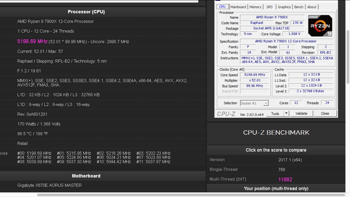
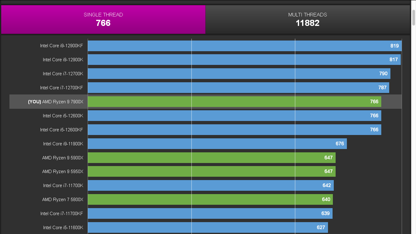
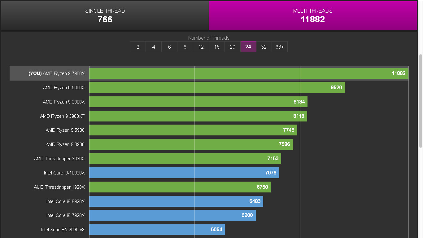
An AMD Ryzen 9 7900X 12-core/24-thread processor sample was put through CPU-Z Bench, the internal benchmark of the app. The chip boosted up to 5.20 GHz in the test, and ran at temperatures as high as 86°C, as reported by CPU-Z. It scored 766 points in the single-threaded test, and 11882 points in the multi-threaded one. The single-threaded numbers in particular are interesting. 766 points would put the 7900X behind the Core i7-12700K and its "Golden Cove" P-core by around 3%. In the multi-threaded test, however, the 7900X, with its 11822 points, is in the league of the next-generation Core i7-13700K (8P+8E) processor, which was recently spotted scoring 11877 points with a 6.20 GHz overclock. The 7900X will hence be pushed as a superior alternative to the i7-13700K for productivity and creator tasks, whereas its single-threaded score ensures that it falls behind the i7-13700K in gaming by a fair bit.


Sources:
Elchapuzas Informatico, TUM_APISAK (Twitter)

123 Comments on AMD Ryzen 9 7900X CPU-Z Benched, Falls Short of Core i7-12700K in ST, Probably Due to Temperature Throttling
N5 N5P N4 N4P N4X 4N
5 nm process - Wikipedia
Which is proved now to be a lie. It is a scam. :banghead:
The worst thing is that there is NO global agreement between the manufacturers on how to label these manufacturing processes.
So, in the end people get Samsung 5LPE/4LPE to be in the range of TSMC N6 process.
"""The term "3 nanometer" has no relation to any actual physical feature (such as gate length, metal pitch or gate pitch) of the transistors. According to the projections contained in the 2021 update of the International Roadmap for Devices and Systems published by IEEE Standards Association Industry Connection, a 3 nm node is expected to have a contacted gate pitch of 48 nanometers and a tightest metal pitch of 24 nanometers.[14] However, in real world commercial practice, "3 nm" is used primarily as a marketing term by individual microchip manufacturers to refer to a new, improved generation of silicon semiconductor chips in terms of increased transistor density (i.e. a higher degree of miniaturization), increased speed and reduced power consumption,[15][16] Moreover, there is no industry-wide agreement among different manufacturers about what numbers would define a 3 nm node. Typically the chip manufacturer refers to its own previous process node (in this case the 5 nm process node) for comparison."""
3 nm process - Wikipedia
Whether or not it matches a physical feature of the product is utterly irrelevant as long as they're not promising functionality that they can't deliver. That's where calling it a scam falls apart - this isn't selling a 150Hp car engine as being 250Hp, or a 600 lumen light bulb as 1000 lumen. Exact feature sizes of the nodes are utterly and completely irrelevant - it's the performance and characteristics of the node that matters. And the fact that node changes today are smaller than ten or twenty years ago doesn't directly matter to anyone outside of the few thousand chip design engineers in the world - and these people know very, very well what the characteristics of these nodes are. What matters is how actual products perform.
Also: TSMC no longer uses nm or nanometers to designate their nodes, so that part of your argument kind of falls apart, no? They have adopted a fully arbitrary naming scheme that points backwards to previous "XXnm" naming, but makes absolutely zero claims about feature sizes. The same goes for Samsung, and now Intel too. None of this is a scam, as nobody is being promised anything meaningful that they aren't getting. If you feel like you're being promised a 5nm feature size but aren't getting it.... so what? Do you use your chips to actually do things, or are you spending all day looking at them through electron microscopes?
Performance and related traits matter. Feature sizes don't matter outside of how they affect performance and density - and they don't matter at all in an absolute sense, only through how they change things compared to previous and competing nodes.
Yes, the customers do expect some performance, which is not offered by the manufacturer.
For example, how would you explain that "Samsung 3GAE/3GAP" is a crap node in the range of TSMC N4/N4P/N4X and not competitive at all with TSMC' own N3/E nodes which are miles ahead??
Read this:
""OregonLive got a scoop about Intel potentially renaming their 7nm process to 5nm to match the marketing schemes from the foundries. If Intel does this, SemiAccurate feels they are walking into a trap that will accomplish nothing more then making them look worse.
The idea is simple enough, over the past decade or two, process nodes have become completely disentangled from the bonds of reality when it comes to naming. The old micron/nanometer naming convention was based on the smallest line/feature that a node could draw, more or less. Actually lets run with the disclaimer up front, there is a lot of stuff in this article that we will massively oversimplify and some we won’t cover, the broad ideas are what matter, not the technical details. This story is about marketing games that are more or less entirely divorced from anything reality based after all. We will also point out that none of the players in this story have anything close to clean hands.""
Intel should not rename their processes - SemiAccurate
Your second line here perfectly encapsulates the problem with your understanding here. You say "the customer expects some performance" - which is exactly what I'm saying as well. What matters is how the node performs, not what number is on the sticker. Names are arbitrary; performance characteristics are real and meaningful. Customers expect performance increases, and do not care whatsoever about whether or not the smallest feature of the node is actually the same number of nm as the number in the node's name. Why would they care? How would that matter to anyone? Feature sizes in nanometers are not in any way directly related to how a node performs - that's far, far too simplistic - as is aptly demonstrated by the performance differences between different "7nm-class" nodes despite these having relatively well matched feature sizes.
There is literally no reason why names need to have a direct relation to reality. That's not how language works on any level - the representational operations of language are symbolic, not indexical. A name can be literally whatever people agree on it being.Yes, the old naming convention was based on this, as that quote says. But this hasn't been reality for, what, a decade now? And the entire industry has abandoned that practice - first implicitly, then explicitly. Is there some reason why they can't change how they name their products?
What that paragraph argues is that Intel shouldn't rename their process nodes because it would make them look bad, as unlike the other actors in the industry they haven't made as gradual of a shift towards a newer scheme - forcing them to explicitly rename nodes that are already launched. You could make a principled argument of some kind here, but then that would need to apply to literally every node created over the past decade - and it wouldn't matter whatsoever, as their performance would still be the same regardless. Whether TSMC N3 is called N3 or "TSMC 22nm interconnect pitch" is entirely irrelevant to its performance, and thus to customers - beyond the latter being complicated and difficult to deal with as a name. The only circumstances in which this would be anywhere close to a scam is if they were promising performance improvements that they aren't delivering.
What it is, is an improved library on N5. In old intel parlance it would be N5+. Keep in mind these are not nanometers, these are like model numbers.
N3 is a little bit better than a half node shrink vs N5, it is not a full node shrink though. In fact I believe the newer "N3E" is actually less dense than the N3 node, but allows for higher power. i.e. it is a library adjustment again.
3nm Technology - Taiwan Semiconductor Manufacturing Company Limited (tsmc.com)
But nvidia is run by lunatics, while AMD is run by lazy who will lag behind until 2025.
Let's be extremely generous and assume the N3 "H2 2022" date means July 1st. And let's be even more absurdly generous and say it took TSMC three months to have significant spare N3 capacity that Apple either didn't want or didn't have an option to buy first. That would place the start of GPU die mass production on October 1st. Processing a single wafer takes ~1 month (a bit less on some processes, more on others). Let's assume TSMC had 10 000 wafer starts/month of free N3 capacity (which is likely closer to their total N3 capacity that early), and that they all went into producing a 3nm AD102. Assuming perfect scaling, that would be a ~375mm2 die (using scaling numbers from here). Let's assume the chip is a bit rectangular, something like 15*25mm. Assuming the "N7 standard" 0.09 defects/cm2 - which is again highly unlikely this early in mass production of a new node, and thus a very generous assumption - and plugging those numbers into a wafer yield calculator, that gives us 101 good dice per wafer, and 39 defective dice, the majority of which can likely be used for a cut-down SKU. Let's say they get 130 RTX 4090-capable dice out of each wafer. That gives us 1.3M GPU dice after a month of production. Which sounds like a lot! Except that every single assumption made in this calculation is wildly unrealistic.
- Apple most likely has 6 months or more exclusive access to N3 mass production, and past any exclusivity period they will have first purchasing rights to any spare capacity
- Even disregarding that, there is no way there are 10 000 available wafer starts after three months for Nvidia - 10% of that is more likely, if not even less.
- This all assumes that the chip is already fully taped out and has had test production runs so that the ramp to mass production is smooth.
- N3 yields are likely significantly lower than 0.09 defects/cm2 this early in mass production.
And, crucially, the die being done doesn't mean it's ready to go on shelves - the wafers need to be shipped to a packaging plant where the wafer is cut, the dice are tested, binned and packaged. The packaged dice are then sold and shipped on to AIB partners, who - again, assuming they've had sufficient access to ES silicon - will then ramp mass production of GPU PCBs and coolers (some of this might be made ahead of time, but these companies generally don't have the cash flow to keep significant parts stock for long periods of time). Then the finished GPUs need to go through QC, testing and retail packaging, before being shipped to distribution centers and then shipped across the globe. This is, at best, a 4-6 month process from a wafer starts processing till the finished product reaches retail shelves. Assuming everything goes smoothly. So, even with wildly unrealistic base assumptions, Nvidia would in a best case scenario be able to launch the 4000 series on N3 somewhere in the early February - late March 2023 timeframe. With any kind of realistic assumptions, we'd be talking H2 2023, if not later. That's a full year's delay, not "several months".