Saturday, March 25th 2023

Intel LGA 7529 Socket Photographed Again, Comparisons Show Gargantuan Physical Footprint
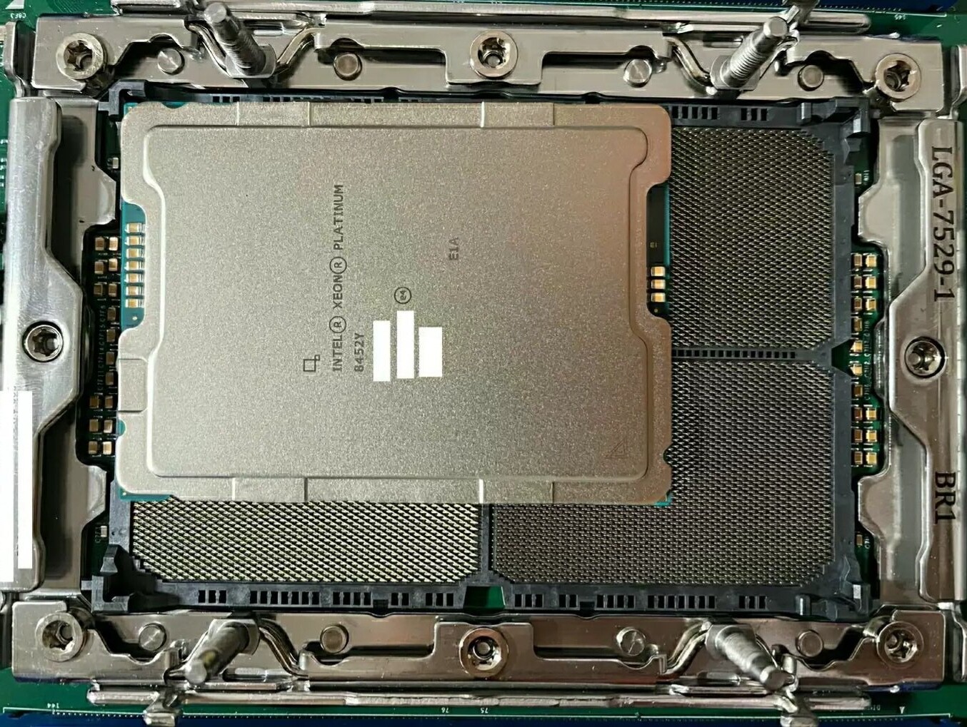
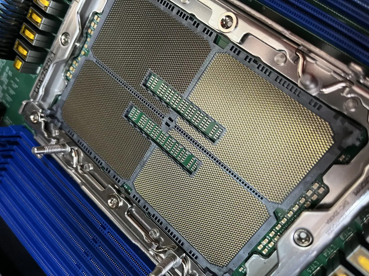
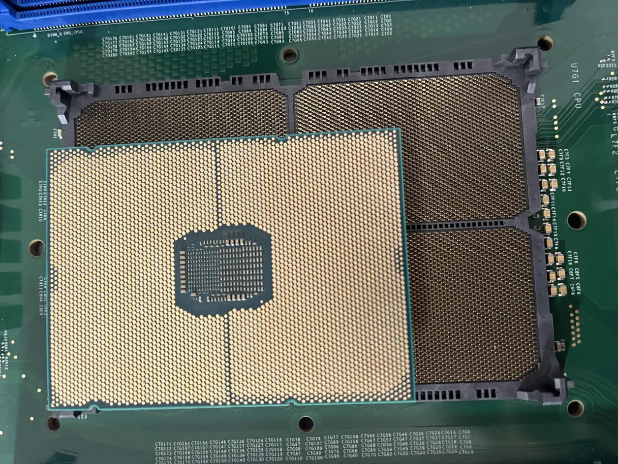
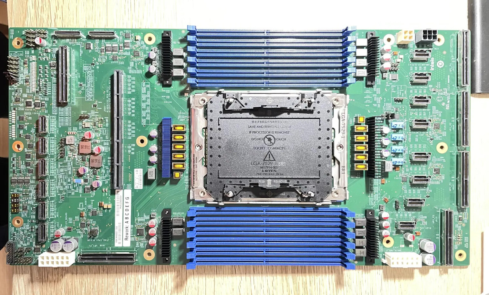
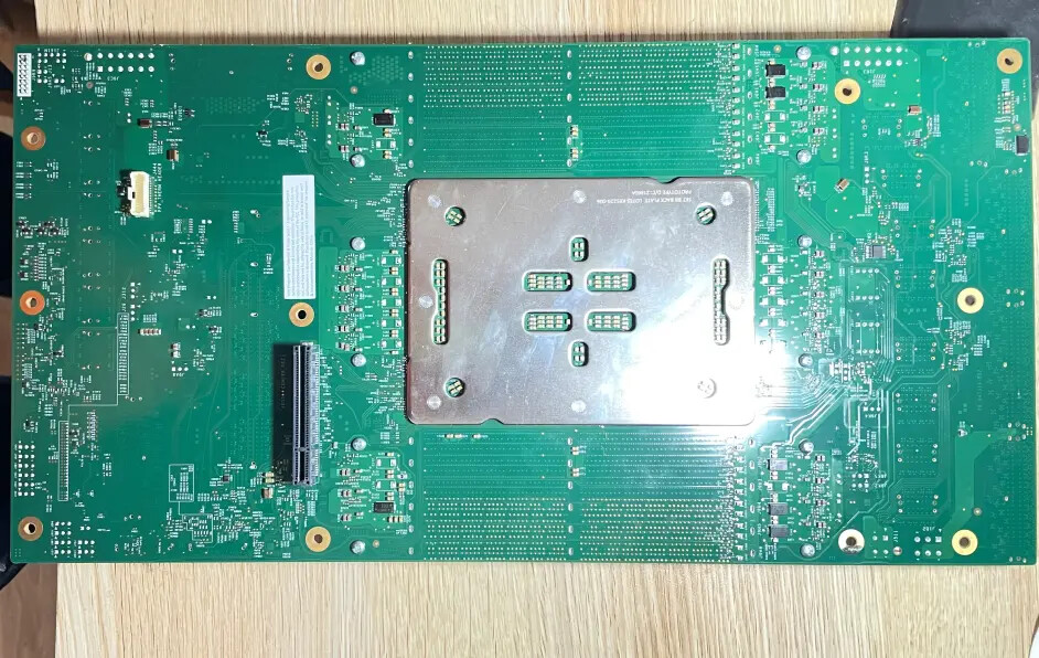
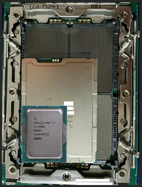
A set of detailed photos has been uploaded to a blog on the Chinese Bilibili site, and the subject matter is an engineering sample of a motherboard that features Intel's next generation LGA 7529 socket. Specifications and photos relating to this platform have cropped up in the past, but the latest leak offers many new tidbits of information. The Bilibili blogger placed a Sapphire Rapids Xeon Processor on top of the the new socket, and this provides an interesting point of reference - it demonstrates the expansive physical footprint that the fifth-generation platform occupies on the board.
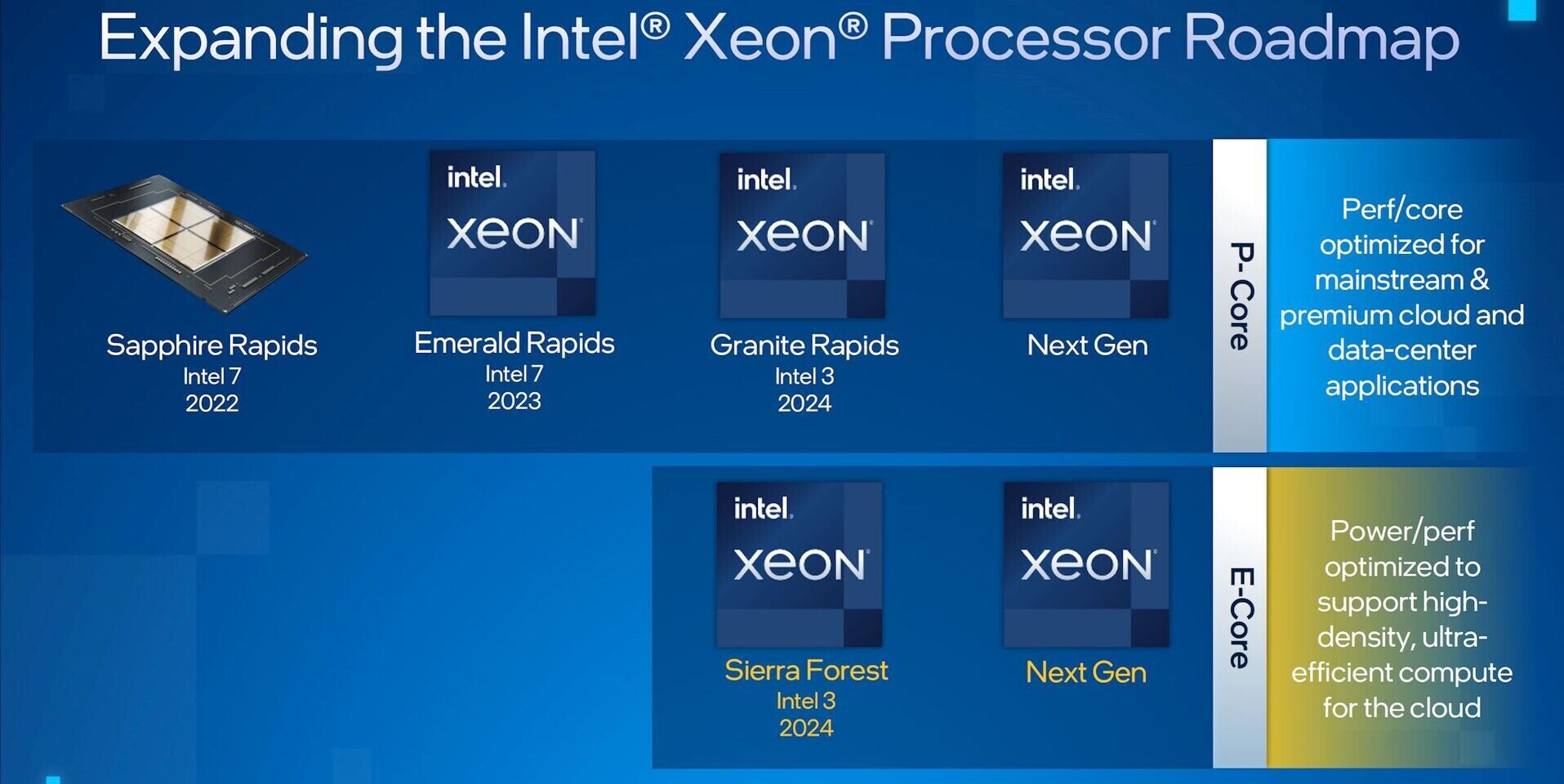
This year's Sapphire Rapids LGA 4677 (Socket E) is already considered to be a sizeable prospect - measuring at 61 × 82 mm. The upcoming Mountain Stream platform (LGA 7529) is absolutely huge in comparison, with eyeball estimates placing it possessing rough dimensions (including the retention arm) of 66 × 92.5 mm. The fifth generation platform is designed to run Intel's Granite Rapids and Sierra Forest CPUs - this family of Xeons featuring scalable microarchitecture is expected to launch in 2024. The code name "Avenue City" has been given to a reference platform that features a dual socket configuration.

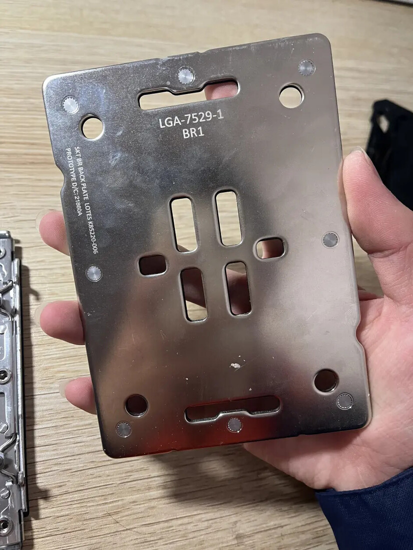
 Based on an analysis of the single socket engineering sample motherboard, the leaker has theorized that this new Xeon platform will offer support for P-Core variants with up to 86 and 132 cores and E-Core variants with up to 334 and 512 cores, as well as HBM variants. The photographed board has "ES" labeled in multiple locations and stamping on the socket indicates that the whole package is a prototype manufactured by LOTES.

 The leaker's findings align with past information that indicated Intel's plans for their forthcoming Granite Rapids and Sierra Forest Xeon processors. These ranges will diverge the Xeon family into two new offerings: one optimized for performance equipped entirely with P-cores, and the other for efficiency equipped with an E-core only array. Industry analysts are proposing that Intel will be targeting the high performance server and cloud computing sectors with these new offerings in 2024.


Sources:
SprayOnCopper Twitter Post, bilibili Blog Entry, harukaze5719 Twitter
This year's Sapphire Rapids LGA 4677 (Socket E) is already considered to be a sizeable prospect - measuring at 61 × 82 mm. The upcoming Mountain Stream platform (LGA 7529) is absolutely huge in comparison, with eyeball estimates placing it possessing rough dimensions (including the retention arm) of 66 × 92.5 mm. The fifth generation platform is designed to run Intel's Granite Rapids and Sierra Forest CPUs - this family of Xeons featuring scalable microarchitecture is expected to launch in 2024. The code name "Avenue City" has been given to a reference platform that features a dual socket configuration.

27 Comments on Intel LGA 7529 Socket Photographed Again, Comparisons Show Gargantuan Physical Footprint
What a beast though :)
First 4 x LGA 7529 socket server prototype...
size DOES matter, hehehe :D
Imagine this kind of CPU in a home workstation or rendering rig. On a 110V you'll need separate circuit breaker just for CPU alone with these things "munching" well over 1kW of power, without any other add-ons in the system. Intel has another P4 moment... multiplied by 20.
For ~10 years now, Intel wins consistently the award for worst CPU retention mechanism in history.
Also, the mobo have so many connection I don't recognize..
The bigger issue (for the entire world) is 12V DC, it's slowly becoming insufficient even in desktops, let alone servers. I think some custom built server and HPC racks already have 48V DC power distribution inside.
No?
Exactly. 18+ phase VRM on consumer boards is completely overkill.
My guess is that they don't have the CPU with the maximum configuration ready yet. Maybe they have one with 100 E-cores or so, and engineering samples run at relatively low speeds anyway, so that modest VRMs are OK for now.
The production version of VRMs should be something like these on the Nvidia H100:
We certainly won't be finding those monster chips used by any except those with very deep pockets like Google, etc.