Wednesday, May 3rd 2023

Intel "Emerald Rapids" Doubles Down on On-die Caches, Divests on Chiplets
Finding itself embattled with AMD's EPYC "Genoa" processors, Intel is giving its 4th Gen Xeon Scalable "Sapphire Rapids" processor a rather quick succession in the form of the Xeon Scalable "Emerald Rapids," bound for Q4-2023 (about 8-10 months in). The new processor shares the same LGA4677 platform and infrastructure, and much of the same I/O, but brings about two key design changes that should help Intel shore up per-core performance, making it competitive to EPYC "Zen 4" processors with higher core-counts. SemiAnalysis compiled a nice overview of the changes, the two broadest points of it being—1. Intel is peddling back on the chiplet approach to high core-count CPUs, and 2., that it wants to give the memory sub-system and inter-core performance a massive performance boost using larger on-die caches.
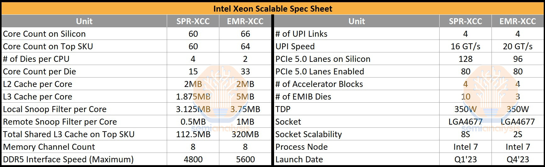
The "Emerald Rapids" processor has just two large dies in its extreme core-count (XCC) avatar, compared to "Sapphire Rapids," which can have up to four of these. There are just three EMIB dies interconnecting these two, compared to "Sapphire Rapids," which needs as many as 10 of these to ensure direct paths among the four dies. The CPU core count itself doesn't see a notable increase. Each of the two dies on "Emerald Rapids" physically features 33 CPU cores, so a total of 66 are physically present, although one core per die is left unused for harvesting, the SemiAnalysis article notes. So the maximum core-count possible commercially is 32 cores per die, or 64 cores per socket. "Emerald Rapids" continues to be based on the Intel 7 process (10 nm Enhanced SuperFin), probably with a few architectural improvements for higher clock-speeds.

 As SemiAnalysis notes, the I/O is nearly identical between "Sapphire Rapids" and "Emerald Rapids." The processor puts out four 20 GT/s UPI links for inter-socket communication. Each of the two dies has a PCI-Express Gen 5 root-complex with 48 lanes, however only 40 of these are wired out. So the processor puts out a total of 80 PCIe Gen 5 lanes. This is an identical count to that of "Sapphire Rapids," which put out 32 lanes per chiplet, 128 in total, but only 20 lanes per die would be wired out. The memory interface is the same, with the processor featuring an 8-channel DDR5 interface, but the native memory speed sees an upgrade to DDR5-5600, up from the present DDR5-4800.
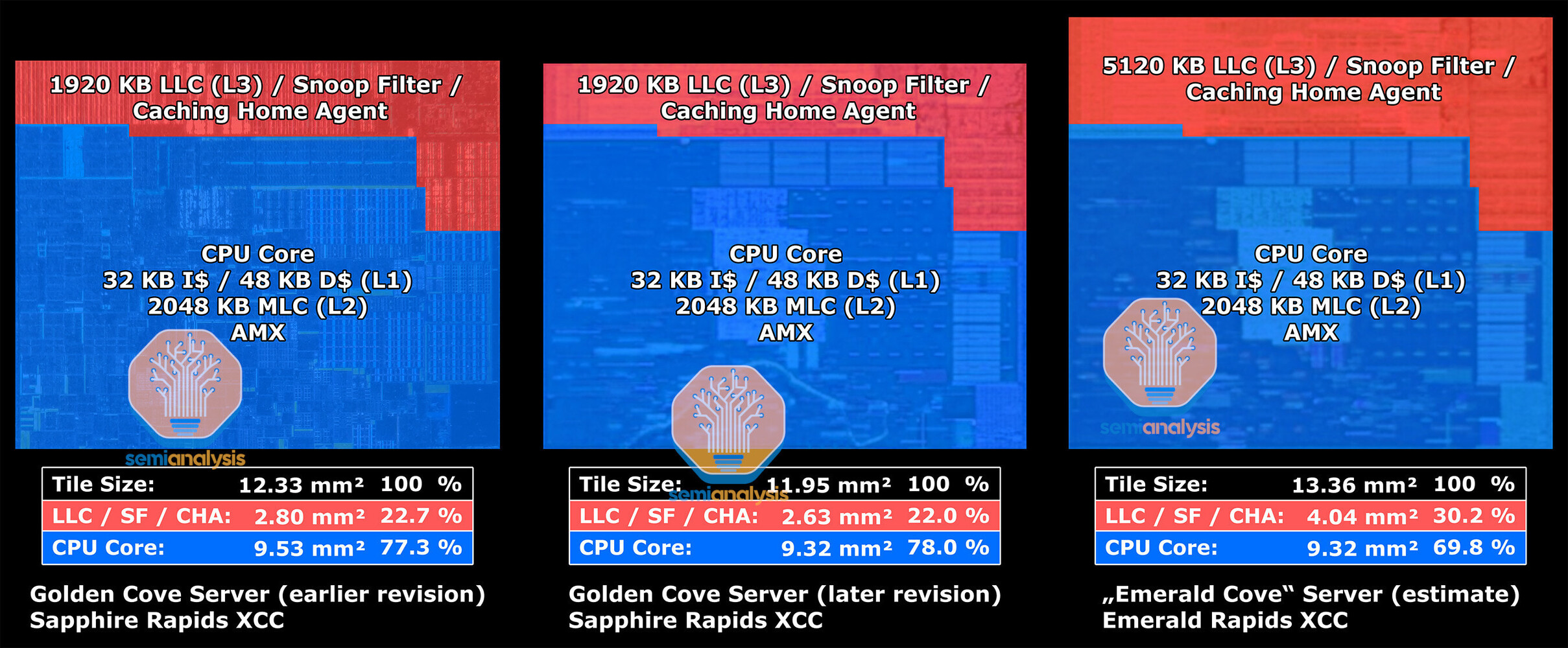
While "Sapphire Rapids" uses enterprise variants of the "Golden Cove" CPU cores that have 2 MB of dedicated L2 caches, "Emerald Rapids" use the more modern "Raptor Cove" cores that also power Intel's 13th Gen Core client processors. Each of the 66 cores has 2 MB of dedicated L2 cache. What's new, according to SemiAnalysis, is that each core has a large 5 MB segment of L3 cache, compared to "Golden Cove" enterprise, which only has a 1.875 MB segment, a massive 166% increase. The maximum amount of L3 cache possible on a 60-core "Sapphire Rapids" processor is 112.5 MB, whereas for the top 64-core "Emerald Rapids" SKU, this number is 320 MB, a 184% increase. Intel has also increased the cache snoop filter sizes per core.
 SemiAnalysis also calculated that despite being based on the same Intel 7 process as "Sapphire Rapids," it would cost Intel less to make an "Emerald Rapids" processor with slightly higher core-count and much larger caches. Without scribe lines, the four dies making up "Sapphire Rapids" add up to 1,510 mm² of die-area, whereas the two dies making up "Emerald Rapids" only add up to 1,493 mm². Intel calculates that it can carve out all the relevant CPU core-count based SKUs by either giving the processor 1 or 2 dies, and doesn't need 4 of them for finer-grained SKU segmentation. AMD uses up to twelve 8-core "Zen 4" CCDs to achieve its 96-core count.
Source:
SemiAnalysis
The "Emerald Rapids" processor has just two large dies in its extreme core-count (XCC) avatar, compared to "Sapphire Rapids," which can have up to four of these. There are just three EMIB dies interconnecting these two, compared to "Sapphire Rapids," which needs as many as 10 of these to ensure direct paths among the four dies. The CPU core count itself doesn't see a notable increase. Each of the two dies on "Emerald Rapids" physically features 33 CPU cores, so a total of 66 are physically present, although one core per die is left unused for harvesting, the SemiAnalysis article notes. So the maximum core-count possible commercially is 32 cores per die, or 64 cores per socket. "Emerald Rapids" continues to be based on the Intel 7 process (10 nm Enhanced SuperFin), probably with a few architectural improvements for higher clock-speeds.


While "Sapphire Rapids" uses enterprise variants of the "Golden Cove" CPU cores that have 2 MB of dedicated L2 caches, "Emerald Rapids" use the more modern "Raptor Cove" cores that also power Intel's 13th Gen Core client processors. Each of the 66 cores has 2 MB of dedicated L2 cache. What's new, according to SemiAnalysis, is that each core has a large 5 MB segment of L3 cache, compared to "Golden Cove" enterprise, which only has a 1.875 MB segment, a massive 166% increase. The maximum amount of L3 cache possible on a 60-core "Sapphire Rapids" processor is 112.5 MB, whereas for the top 64-core "Emerald Rapids" SKU, this number is 320 MB, a 184% increase. Intel has also increased the cache snoop filter sizes per core.

24 Comments on Intel "Emerald Rapids" Doubles Down on On-die Caches, Divests on Chiplets
Also same die process, barely any increase in cores and only 2S doesn’t bode well so soon after Sapphire Rapids launch. Where is Aurora by the way?!?!
cashcache! o_OWhen in ordinary costumers segment?
Intel might have the same issues when going through one CPU die to another, but who knows.
I expect the extra cache and reduced number of dies will help in workloads that are highly threaded but also highly sensitive to core-to-core latency. That's an area I would expect Epyc to struggle with since Epyc has more core dies and nothing like EMIB for connecting them.
Besides i suspect for those workloads lower core count Epyc variants are better anyways due to less chiplets and higher clock speeds.
There are multiple problems with a single large cache, the first of which is that a single large cache is going to be much slower than a bunch of small caches (not that X3D cache is small, just in comparison to if you had added them together).
The 2nd bigger problem is that having a single large cache means that all the chips would have to fetch data from said cache. This is a problem design wise as not every chip is going to be equal distance from said cache and thus latencies increase the further away from the cache you get. You can see with RDNA2 and RDNA3 that AMD puts the L3 cache at both the top and bottom of the chip (whether that be on die or in the form of chiplets) in order to ensure a lower overall latency.
Having a 3D Cache chip on each CCD is vastly superior because it means that each CCD can localize all the data needed for work to be performed. The chiplet isn't wasting time and energy fetching data off die because it doesn't need to. We can see this from the energy efficiency of Zen 4 X3D chips and their performance in latency critical applications. In addition, due to how AMD stacks it's L3 on top you can put a ton of cache onto a chip while maintaining a lower latency that would otherwise be impossible if you tried to fit that cache onto a single chip. Now instead of a wire running halfway cross the chip on the X axis, you have a much smaller wire running on the Y axis.
So long as Intel isn't stacking it's cache AMD has an advantage in that regard.
I think you haven't thought of the coherence problem as say CORE#0 in Chiplet #0 has written something in Memory Address #XYZ, ofc, as per hierarchy it is first written to L1 and could eventually propagate in the hierarchy.
CORE#32 in Chiplet#5 wants to access the data in that same address. If L1/L2/L3(one of or more if inclusive) of CORE#0 still contains the data and hasn't written it to the main memory then that poses a problem as fetching it from the main memory would result in a wrong result. A simple solution would be to implement a write-through mechanism(i.e. you simply write to the memory whatever is written to the cache), but that could cause performance issue, though nothing that a lot of things do need to be written-through(e.g. peripherals that need to be updated now and not 'sometime in the future') so there are options to do it like caches flushes or mapping the same address twice, one passes through cache and other doesn't.
So the way that designers handle it is through bus snooping and/or directories. This shows how hard it is to implement chiplets as a mechanism to keep the coherence between the two or more really isn't going to be easy and should be the reason why CCD-to-CCD communication is very slow(it even shares the same 32B/cycle infinity fabric link that the CCD uses to communicate with the rest of the system, specially memory and really one of the big reasons why increasing IF clocks can improve perf in AMD processors).
That's not saying that Intel doesn't have a lot of challenges with L3 implementations and stuff. Alder Lake itself is known to reduce the ringbus clocks(same as L3 clocks) to the Gracemont cores when those are active, effectively slowing down the Goldmont cores L3 slices.RDNA2/3 cache isn't the exact same. Specially for RDNA3 where they are together with the memory controller and so don't have a coherence problem, as it can only contain data specific to each memory controller. Probably one of the reasons why infinity cache is faster in RDNA3.
www.anandtech.com/show/17585/amd-zen-4-ryzen-9-7950x-and-ryzen-5-7600x-review-retaking-the-high-end/10
They call it core-to-core latency but as far as I know, there is no method of directly sending signals or data from one core to another core. Rather, it's the latency when a core attempts to access data that is cached in a known location in the L3, in a slice of cache that belongs to another core. But that's alright, it's what matters here, and the latency across chiplets is ~77 ns.
Applying these numbers, we can estimate that the yield at which all cores in the EMR can be activated is in the 60% range, and if we assume that one core is disabled, the yield is close to 90%.
The fact that Intel 10nm has significantly improved yield was commented on in the Q2 2021 financial report.
Sapphire Rapids was Intel's first wide-release processor using EMIB (I'm not counting Ponte Vecchio because it sells orders of magnitude fewer CPUs than Xeons) and I suspect that they underestimated the cost of EMIB in wide deployment. Probably a combination of (relatively) low yields of chips using EMIB and production bottlenecks due to limited number of facilities that can assemble EMIB chips (compared to the number of 10nm fabs). Having fewer EMIB connections in chips means the existing EMIB facilities can assemble more chips. The tradeoff is a reduction of 10nm wafer yield (due to larger dies), but Intel is probably more equipped to handle the reduction in wafer yield because of the large number of facilities producing 10nm wafers.