Saturday, December 13th 2025

Huawei Ascend 950 AI Accelerator Pictured
Huawei's next-generation Ascend 950 AI accelerator has been pictured for the first time, showcasing the company's custom silicon and HBM memory. The chip combines Huawei's first self-developed HBM memory with a new generation of AI acceleration. Huawei aims to compete through scale rather than focusing solely on single-chip performance. Although it currently trails NVIDIA in per-chip performance, Huawei's system-scale solutions can still be competitive. The company has announced the Ascend 950 family for early 2026, featuring two variants.
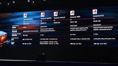
The 950PR model includes 128 GB of in-house HBM with around 1.6 TB/s of bandwidth, while the 950DT model increases memory to 144 GB and boosts bandwidth to nearly 4 TB/s. Both chips target one PetaFLOP of FP8, and two PetaFLOPS of FP4. Huawei's competitive strategy emphasizes dense packaging and aggressive networking, rather than relying solely on raw per-chip performance. We have no information on the node selection, but it will likely be SMIC's newest N+3 node with 5 nm-class features. Chinese SMIC has officially achieved volume production of its newest 5 nm node relying on the deep ultraviolet (DUV) to manufacture its silicon. Since the first customer for N+3 was Huawei with Kirin 9030 SoC, it is only logical that the more important Ascend AI accelerator family is manufactured using the same node.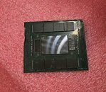
 Examining the chip, we observe two dies combined into a multi-chip module, which includes two additional silicon dies. These likely function as I/O and networking modules, connecting to the massive SuperPoDs and SuperClusters constructed from these components. This is interconnected by a new Lingqu interconnect protocol and optical links designed to connect hundreds of thousands of Ascend 950 cards. Surrounding the bare silico is something resembling the LPDDR/HBM memory hybrid, which is likely Huawei's homegrown HBM memory. The company likely packages these HBM modules as standalone chips, and just stacks them across the package.
Source:
@Jukan05 on X
The 950PR model includes 128 GB of in-house HBM with around 1.6 TB/s of bandwidth, while the 950DT model increases memory to 144 GB and boosts bandwidth to nearly 4 TB/s. Both chips target one PetaFLOP of FP8, and two PetaFLOPS of FP4. Huawei's competitive strategy emphasizes dense packaging and aggressive networking, rather than relying solely on raw per-chip performance. We have no information on the node selection, but it will likely be SMIC's newest N+3 node with 5 nm-class features. Chinese SMIC has officially achieved volume production of its newest 5 nm node relying on the deep ultraviolet (DUV) to manufacture its silicon. Since the first customer for N+3 was Huawei with Kirin 9030 SoC, it is only logical that the more important Ascend AI accelerator family is manufactured using the same node.


4 Comments on Huawei Ascend 950 AI Accelerator Pictured