Tuesday, July 21st 2026

NVIDIA Details the "Rubin" Architecture: Die Annotation, Vera CPU, HBM4, and Disaggregated Inference
NVIDIA has released a technical details on its next-generation "Rubin" GPU, including a fully annotated die shot. "Rubin" represents a significant generational leap in NVIDIA's mission to scale computing across numerous racks, systems, and data centers. The company is promoting this generation as the first "agentic AI" native design. This AI paradigm means that inference workloads are continuously active, engage in reasoning, planning, tool utilization, and execute many sequential steps. In this context, inference refers to a completed model running on the GPUs, rather than being trained, which is what Rubin is designed for. NVIDIA claims up to 10x more agentic throughput per unit of energy compared to "Blackwell." This improvement relies not only on the new "Vera" CPU and rack-level power management but also on the entire system, as customers now prioritize overall system performance rather than just the performance of a single GPU.
In its full configuration, "Rubin" combines two compute dies in a single package, linked with a high-speed connection that NVIDIA calls NV-HBI. This chiplet approach uses CoWoS-L packaging from TSMC, chosen because each die is already as large as the chip factory can print in one go, reaching the reticle limit. The GPU contains 336 billion transistors, up to 224 SMs, 896 Tensor Cores with a third-generation Transformer Engine, and 288 GB of HBM4 memory, capable of delivering up to 50 PetaFLOPS of inference and about 35 PetaFLOPS of training at the ultra-compact NVFP4 format. This is NVIDIA's proprietary 4-bit data format that enhances efficiency in inference and training with minimal to no accuracy loss compared to the 8-bit and 16-bit data formats used today for training and inference. However, this is quite different from the FP16/FP32 formats used in gaming GPUs. Below, we will break down not just the GPU, but the entire platform NVIDIA has built around it.
 Inside the GPU
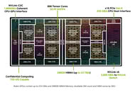 To turn this massive 336 billion transistor budget into sustained throughput, NVIDIA organizes GPU resources into Graphics Processor Clusters (GPCs) built around the 224 SMs. All of these SMs are served by a centralized L2 cache. Working alongside the GPCs is the GigaThread Engine, which coordinates workflows and optimizes GPU resource utilization. There are also MIG Control partitions that enable the GPU to be divided into multiple virtual GPUs, an NVDEC block for accelerated video decoding, and Confidential Computing with TEE-I/O to keep data protected at rest, in transit, and in use. The annotated die shot NVIDIA released puts all of these blocks in context, with the two compute dies mirrored across the NV-HBI link and the HBM4 stacks flanking each die. The system recognizes this dual-die solution as one large GPU.
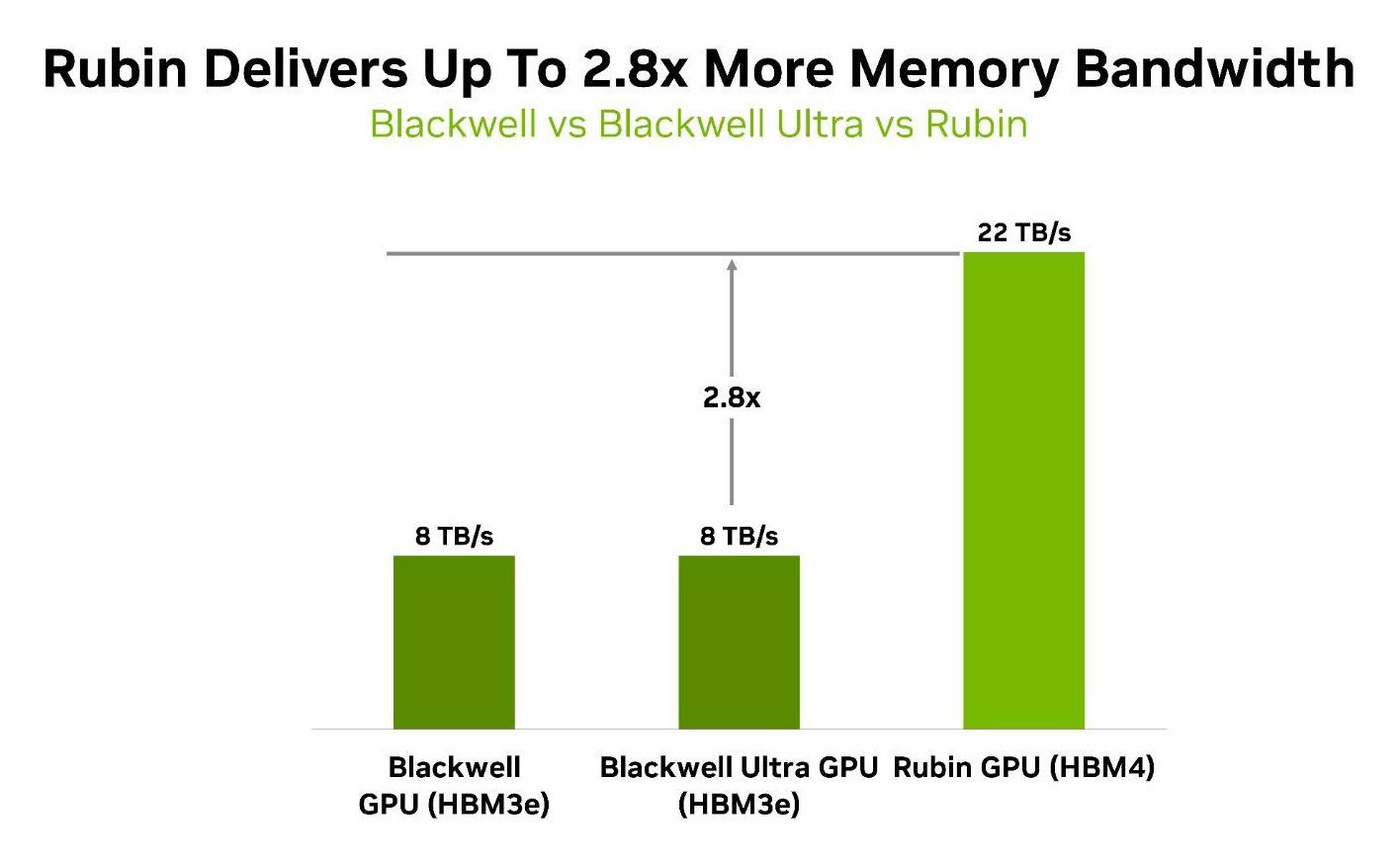
Memory and Interconnect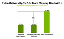 On the memory side, NVIDIA has worked with its memory partners to provide 288 GB of HBM4 memory using 12-high stacks. HBM4 offers up to 22 TB/s of peak memory bandwidth, a 2.8 times increase over both "Blackwell" and "Blackwell Ultra," which top out at 8 TB/s. For reference, a GeForce RTX 5090 with its GDDR7 memory delivers less than 2 TB/s. This increase is partly due to HBM4 doubling the interface width compared to HBM3E, with the rest coming from more memory driving higher bandwidth. The Tensor Memory Accelerator (TMA) has been updated to move data more efficiently. The NVLink 6 update manages the integration of the GPU into the rest of the rack for scale-up domains. This communication is crucial for getting the GPUs inside the rack to function as one. With NVLink 6, all-to-all GPU communication operates on 3,600 GB/s of fabric bandwidth, while NVLink-C2C chip-to-chip enables coherent CPU-GPU communication at 1,800 GB/s. NVIDIA also includes a x16 PCIe Gen 6 host interface with up to 256 GB/s of bandwidth for communication with the CPU and external devices.
Tensor Cores, Sparsity, and Attention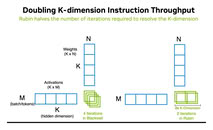 Beyond raw throughput, NVIDIA has tuned "Rubin" for the specific bottlenecks of inference. The redesigned Tensor Cores, working with the third-generation Transformer Engine, double throughput per clock by processing twice as much data along the K (reduction) dimension. In practice, a matrix multiply that needs four K-loop iterations on "Blackwell" finishes in two on "Rubin"—handy when a model is split across many GPUs and each one handles a large reduction dimension.
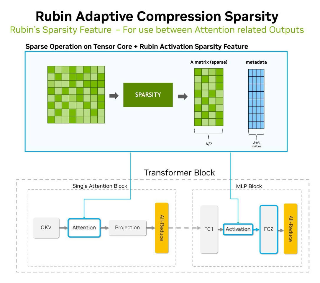
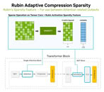 "Attention" is the math that lets a language model weigh how much each word relates to every other word, and it is one of the heaviest parts of running long prompts. For this long-context attention, "Rubin" can load the intermediate attention scores into a structured 2:4 sparse compressed form—effectively skipping half the values that contribute little—cutting the work done in softmax and the second attention matrix multiply while preserving a dense output. Softmax throughput also rises, with NVIDIA quoting 2x FP32 and 4x BF16/FP16 exponential throughput versus the "Blackwell" baseline.
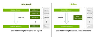 There is also a specific win for mixture-of-experts (MoE) models, the design behind most of today's largest LLMs. Rather than one giant dense network where every parameter runs on every token, an MoE model is split into many smaller sub-networks called "experts," and a lightweight router picks just a few of them for each token. Only a fraction of the model activates at any moment, which is how a model can carry trillions of parameters yet stay affordable to run. The catch is that every active expert needs its own weights streamed to the Tensor Cores, and describing those transfers to the TMA normally means one descriptor per expert—metadata that piles up as expert counts climb into the hundreds. Rubin's enhanced TMA lets a single descriptor be shared across all experts that use the same layout, cutting that overhead.
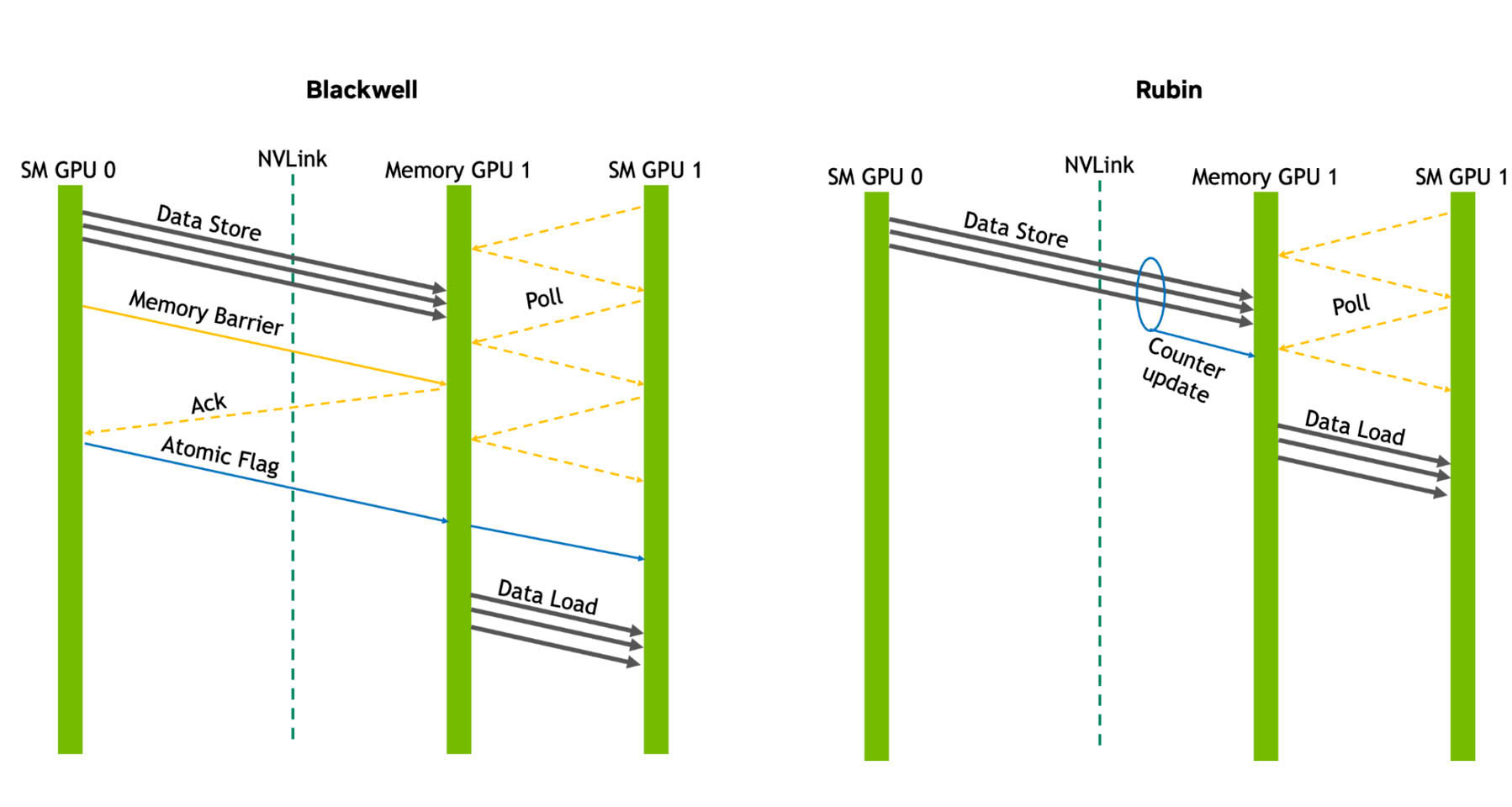
Scale-up Communication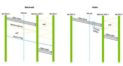 One of NVIDIA's biggest advantages is scale-up communication—letting a GPU exchange data with the others in its rack without stalling. The traditional way to keep two GPUs in sync is a barrier, or handshake. The sender writes its data, then raises a flag; the receiver waits at the barrier, checks that flag, and often sends an acknowledgment back before it can safely read. Every one of those steps is a round-trip, and the cost climbs as more GPUs pile into the same exchange—the system ends up spending more time coordinating than computing.
"Rubin" replaces that with "counted writes" for device-initiated NVLink transfers. Instead of a flag-and-acknowledge handshake, each incoming write simply bumps a counter on the receiving GPU, and the consumer waits for that counter to reach the number of writes it is expecting before it starts reading. Think of tracking a delivery: rather than calling the sender to confirm each package, you ordered eight, watch the counter tick to eight, and get to work. "Transfer finished" and "safe to read" collapse into one cheap check.
Why it is a clever fix comes down to three things. It is device-initiated, so each GPU drives its own transfers without waiting on the CPU to orchestrate them. It removes the back-and-forth acknowledgment traffic that clogs large all-to-all exchanges. And because reading a counter is so lightweight, it scales cleanly as GPU counts climb—exactly the regime a 72-GPU rack lives in—keeping the compute pipelines full instead of idling on synchronization.
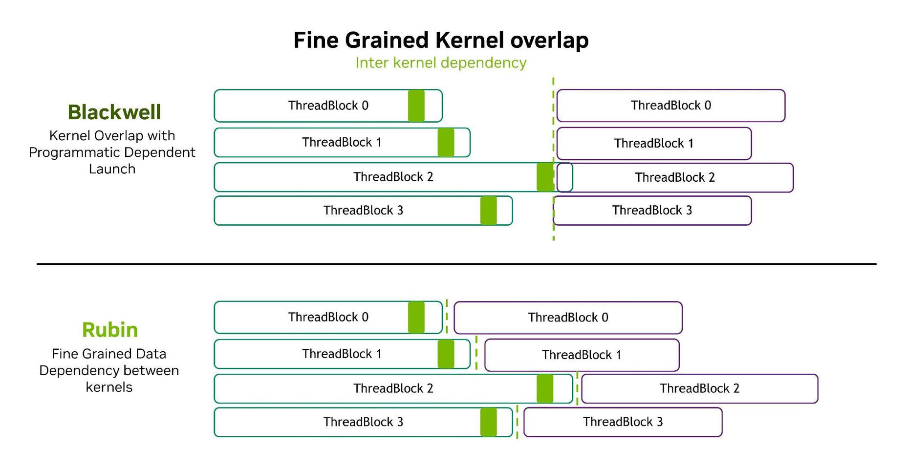
Fine-grained Kernel Overlap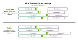 NVIDIA has also worked to keep the GPU's execution timeline tightly packed. In inference, one kernel (a single GPU program) often produces data that the next kernel immediately consumes, and any gap between them shows up directly as lost tokens per second—the AI equivalent of frametime stuttering. "Blackwell" reduced these bubbles with programmatic dependent launch, but a consuming kernel could still stall waiting on a broad dependency. "Rubin" moves to finer-grained, tile-level triggering, so a consumer kernel can begin as soon as the specific data it needs becomes available, rather than waiting for the entire producer kernel to finish.
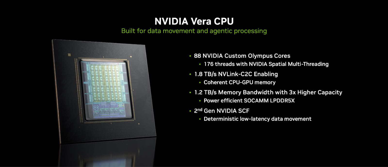
The CPU Half of the Superchip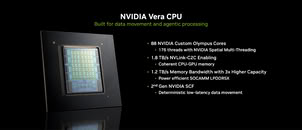 "Rubin" never ships alone—it is one half of the "Vera Rubin" superchip, paired with NVIDIA's first fully in-house CPU, "Vera." Built from 88 custom-designed "Olympus" cores (176 threads), it connects to its two Rubin GPUs over the 1,800 GB/s coherent NVLink-C2C link mentioned above and handles the control-heavy, latency-sensitive orchestration that keeps the GPUs fed. Olympus is still an Arm design—it stays Armv9.2-compatible, so existing Arm software runs unchanged—but where the previous "Grace" CPU used Arm's off-the-shelf Neoverse cores, "Vera" is NVIDIA's own from-scratch core, giving it full control over the design. We covered the full "Vera" specifications when NVIDIA launched it.
"Rubin CPX" and Disaggregated Inference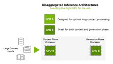 NVIDIA also splits inference itself across two different chips. Modern reasoning models divide a request into a compute-heavy "context" (prefill) phase, where millions of input tokens are processed at once, and a bandwidth-heavy "decode" (generation) phase, where tokens are produced one at a time. Running both on the same expensive HBM-equipped GPU wastes silicon, so NVIDIA built a dedicated companion: "Rubin CPX." It is a monolithic, single-die accelerator delivering 30 PetaFLOPS of NVFP4 compute paired with 128 GB of the far cheaper GDDR7 memory—no CoWoS packaging and no HBM required—plus four NVENC and four NVDEC units—the same fixed-function video codec blocks found on GeForce cards—to cheaply decode the hours of video that can make up a long context, rather than still images. In the "Vera Rubin NVL144 CPX" rack, CPX chips handle the context phase while the HBM4-equipped Rubin GPUs handle decode, and the combined platform targets 8 ExaFLOPS of NVFP4 compute, 100 TB of fast memory, and 1.7 PB/s of aggregate bandwidth. We covered the CPX reveal in more detail when it was first announced.
Power and Rack Scale
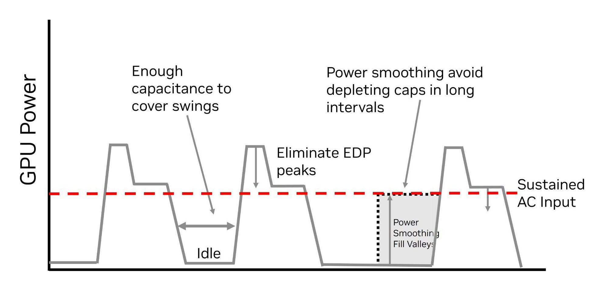
These systems consume significant power. Everything ships as a single rack, an enclosure roughly the size of a large refrigerator, holding 72 Rubin GPU packages wired together so software treats them as one enormous GPU. NVIDIA now also markets that as "NVL144," since it counts each package's two compute dies as an individual GPU.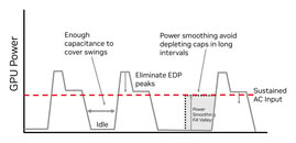 For the "Vera Rubin" NVL72, NVIDIA developed Intelligent Power Smoothing to bring every system component under a single fixed power envelope. During AI workloads, power demand can swing rapidly, from idle GPUs waiting on a CPU to full utilization. Anyone who has watched a GPU trip a power supply's protection with a sudden transient spike will recognize the problem, just scaled up to an entire room. Using state-of-charge power smoothing, "Vera Rubin" NVL72 reduces average power consumption by approximately 10% and 50 ms peak power by about 20% compared to previous-generation techniques.
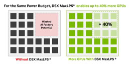 Power budget optimization is further enhanced at the AI-factory level with NVIDIA DSX MaxLPS, which NVIDIA says can let operators provision up to 40% more GPUs within the same power budget. The rack uses a third-generation MGX design with cable-free compute and switch trays, 45°C liquid cooling, hot-swappable NVLink switch trays, and open connectivity across NVLink and Spectrum-X Ethernet. That 45°C coolant is warm by design. It is still far cooler than the roughly 90°C chips, so it pulls heat away just fine, yet it is hot enough to be dumped straight outdoors with simple dry coolers year-round—no power-hungry chillers making cold water the silicon never needed. Staying warm also keeps the loop above the dew point, so no condensation forms on the hardware.
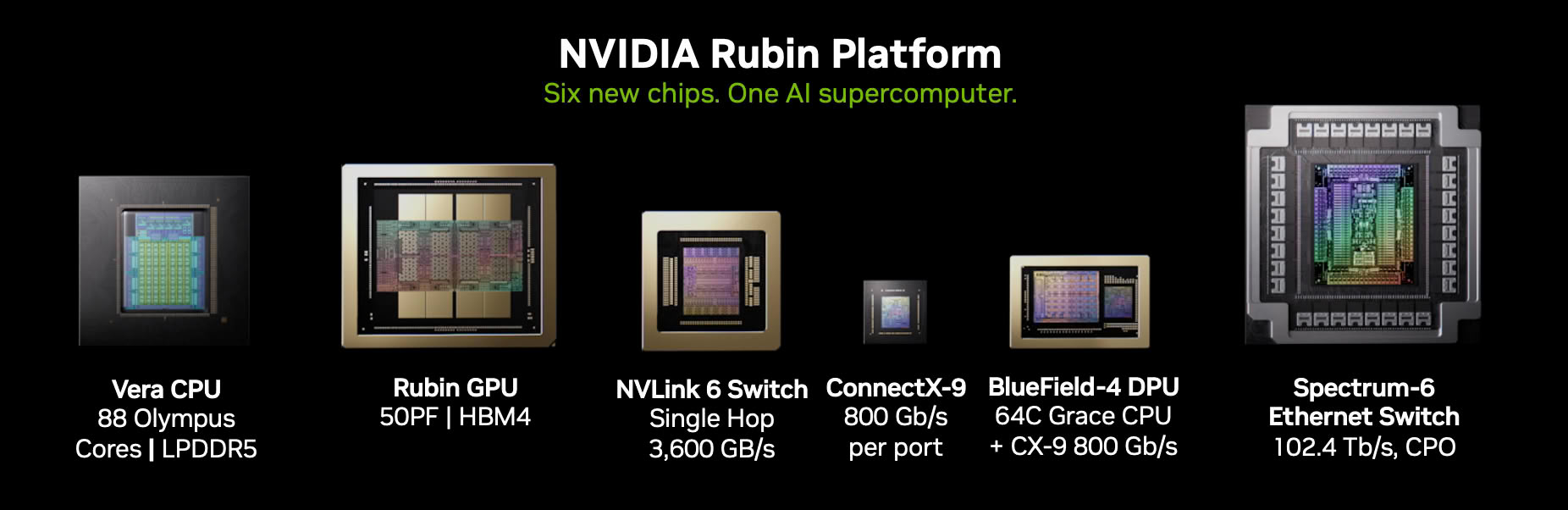
One Platform, Six Chips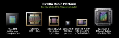 It is worth stressing that "Rubin" is only the most visible piece of a six-chip platform NVIDIA designed together: the "Rubin" GPU and "Vera" CPU are joined by the "Rubin CPX" inference accelerator, the NVLink 6 Switch (3.6 TB/s of bidirectional bandwidth per GPU across a full all-to-all topology of 72 GPUs), the ConnectX-9 SuperNIC (800 Gbit/s per port, up to 1.6 Tbit/s of scale-out networking per GPU), the BlueField-4 DPU for networking, storage, and security offload, and the Spectrum-6 Ethernet switch (102.4 Tbit/s of total switching with co-packaged silicon photonics). NVIDIA expects the "Vera Rubin" NVL72 to reach mass production in the second half of 2026, with the "Rubin CPX" configurations following later in the year.
Source:
NVIDIA
In its full configuration, "Rubin" combines two compute dies in a single package, linked with a high-speed connection that NVIDIA calls NV-HBI. This chiplet approach uses CoWoS-L packaging from TSMC, chosen because each die is already as large as the chip factory can print in one go, reaching the reticle limit. The GPU contains 336 billion transistors, up to 224 SMs, 896 Tensor Cores with a third-generation Transformer Engine, and 288 GB of HBM4 memory, capable of delivering up to 50 PetaFLOPS of inference and about 35 PetaFLOPS of training at the ultra-compact NVFP4 format. This is NVIDIA's proprietary 4-bit data format that enhances efficiency in inference and training with minimal to no accuracy loss compared to the 8-bit and 16-bit data formats used today for training and inference. However, this is quite different from the FP16/FP32 formats used in gaming GPUs. Below, we will break down not just the GPU, but the entire platform NVIDIA has built around it.


Memory and Interconnect
Tensor Cores, Sparsity, and Attention


Scale-up Communication
"Rubin" replaces that with "counted writes" for device-initiated NVLink transfers. Instead of a flag-and-acknowledge handshake, each incoming write simply bumps a counter on the receiving GPU, and the consumer waits for that counter to reach the number of writes it is expecting before it starts reading. Think of tracking a delivery: rather than calling the sender to confirm each package, you ordered eight, watch the counter tick to eight, and get to work. "Transfer finished" and "safe to read" collapse into one cheap check.
Why it is a clever fix comes down to three things. It is device-initiated, so each GPU drives its own transfers without waiting on the CPU to orchestrate them. It removes the back-and-forth acknowledgment traffic that clogs large all-to-all exchanges. And because reading a counter is so lightweight, it scales cleanly as GPU counts climb—exactly the regime a 72-GPU rack lives in—keeping the compute pipelines full instead of idling on synchronization.
Fine-grained Kernel Overlap
The CPU Half of the Superchip
"Rubin CPX" and Disaggregated Inference

Power and Rack Scale
These systems consume significant power. Everything ships as a single rack, an enclosure roughly the size of a large refrigerator, holding 72 Rubin GPU packages wired together so software treats them as one enormous GPU. NVIDIA now also markets that as "NVL144," since it counts each package's two compute dies as an individual GPU.

One Platform, Six Chips
11 Comments on NVIDIA Details the "Rubin" Architecture: Die Annotation, Vera CPU, HBM4, and Disaggregated Inference
But no, 2040 perhaps...ever, without tricks. Gamers made NV back in the day. NV have dumped us mostly. 🤮
I don't blame them. That's where the profits are. Day dreaming I was.
{Edit due to typo.}