Monday, October 26th 2026

TSMC A14 Node to Break Eight Years of SRAM Scaling Stagnation
TSMC, the world's largest and most advanced semiconductor manufacturer, has been grappling with stagnant progress in SRAM scaling for years. Since the launch of the N5 5 nm process in 2020, the size of the SRAM 6T bitcell has remained around 0.021 µm². While transistor density in logic elements has increased, memory has not seen similar advancements. However, with the introduction of the A14 node, set for production in 2028, TSMC's 6T SRAM bitcell is expected to shrink significantly to 0.017 µm², marking a 19% reduction. This breakthrough indicates that TSMC has successfully advanced the technology and is ready to bring it to mass production with the A14 node.
TSMC is currently conducting pilot production to assess the viability of this semiconductor node, enabling customers to evaluate how their designs will perform in TSMC's production environment. The progress of the A14 node production is promising, with timelines advancing due to early successes. If pilot production continues smoothly without major yield or production issues, risk production is set to commence in 2027, followed by high-volume manufacturing in 2028. If no significant challenges arise next year, TSMC may even accelerate the production schedule by a few months.
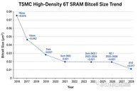 Compared to the recently announced volume production of the N2 2 nm node, the A14 process offers up to 15% higher speeds at the same power level or up to 30% power reduction at the same frequency. TSMC also claims a 20% increase in logic density, alongside a notable 19% improvement in SRAM density. This advancement marks a significant step forward, as logic components and memory are now scaling more effectively with larger jumps between nodes, a contrast to the previous sub-10 nm era. The A14 node will first be implemented in Taiwan at TSMC's main headquarters, where the company plans to begin mass production in 2028.
Source:
ETNews
TSMC is currently conducting pilot production to assess the viability of this semiconductor node, enabling customers to evaluate how their designs will perform in TSMC's production environment. The progress of the A14 node production is promising, with timelines advancing due to early successes. If pilot production continues smoothly without major yield or production issues, risk production is set to commence in 2027, followed by high-volume manufacturing in 2028. If no significant challenges arise next year, TSMC may even accelerate the production schedule by a few months.


3 Comments on TSMC A14 Node to Break Eight Years of SRAM Scaling Stagnation
I expect Samsung to hit 0.018 µm² late 2027