Report an Error


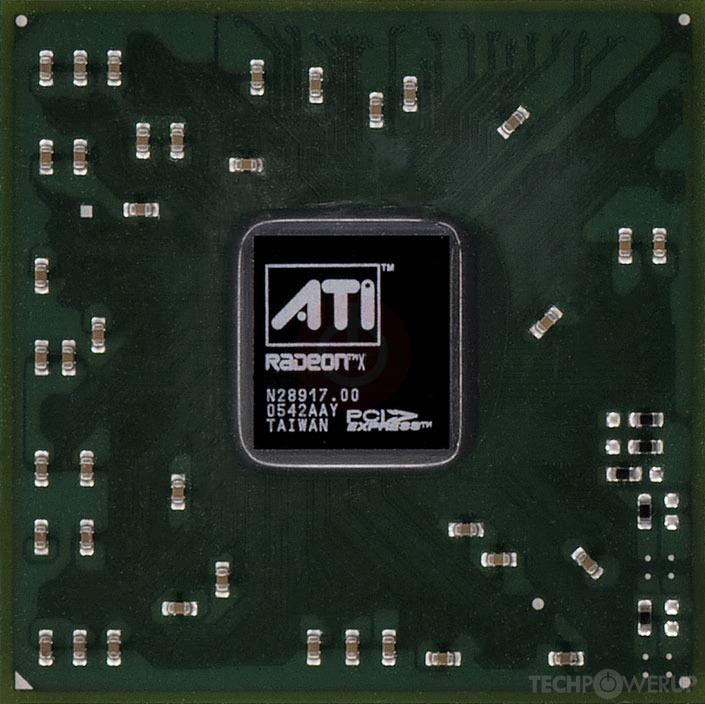
ATI RV370
RV370

RV370 GL
RV370 PRO

RV370 X600 SE
ATI's RV370 GPU uses the R300 architecture and is made using a 110 nm production process at TSMC. With a die size of 74 mm² and a transistor count of 107 million it is a very small chip. RV370 supports DirectX 9.0. Modern GPU compute technologies are not available. It features 4 pixel shaders and 2 vertex shaders, 4 texture mapping units and 4 ROPs. Due to the lack of unified shaders you will not be able to run recent games at all (which require unified shader/DX10+ support).
Graphics Processor
- Released
- Sep 1st, 2004
- GPU Name
- RV370
- Mobile Variant
- M22
- Codename
- Hari
- Architecture
- R300
- Foundry
- TSMC
- Process Size
- 110 nm
- Transistors
- 107 million
- Density
- 1.4M / mm²
- Die Size
- 74 mm²
Graphics Features
- DirectX
- 9.0
- OpenGL
- 2.0
- OpenCL
- N/A
- Vulkan
- N/A
- Pixel Shader
- 2.0
- Vertex Shader
- 2.0
- WDDM
- 1.0
- Compute
- GFX2
Render Config
- Pixel Shaders
- 4
- Vertex Shaders
- 2
- TMUs
- 4
- ROPs
- 4
- Max. TDP
- 36 W
All R300 GPUs
ATI GPU Architecture History
Graphics cards using the ATI RV370 GPU
| Name | Chip | Memory | Shaders | TMUs | ROPs | GPU Clock | Memory Clock |
|---|---|---|---|---|---|---|---|
| RV370 AIW | 256 MB | 4 / 2 | 4 | 4 | 400 MHz | 300 MHz | |
| RV370 LE | 128 MB | 4 / 2 | 4 | 4 | 400 MHz | 250 MHz | |
| RV370 X300 | 64 MB | 4 / 2 | 4 | 4 | 375 MHz | 200 MHz | |
| RV370 SE | 64 MB | 4 / 2 | 4 | 4 | 325 MHz | 200 MHz | |
| RV370 LE | 64 MB | 4 / 2 | 4 | 4 | 325 MHz | 200 MHz | |
| 128 MB | 4 / 2 | 4 | 4 | 325 MHz | 300 MHz | ||
| RV370 PRO | 256 MB | 4 / 2 | 4 | 4 | 400 MHz | 250 MHz | |
| RV370 X1050 | 128 MB | 4 / 2 | 4 | 4 | 400 MHz | 333 MHz | |
| RV370 GL | 128 MB | 4 / 2 | 4 | 4 | 391 MHz | 196 MHz | |
| 128 MB | 4 / 2 | 4 | 4 | 324 MHz | 196 MHz | ||
| 256 MB | 4 / 2 | 4 | 4 | 400 MHz | 250 MHz | ||
| RV370 X600 SE | 128 MB | 4 / 2 | 4 | 4 | 325 MHz | 250 MHz | |
| RV370 PRO | 128 MB | 4 / 2 | 4 | 4 | 400 MHz | 300 MHz |


RV370 GPU Notes
| Mobile Variant: M22 Codename: Hari Graphics/Compute: GFX2 Smart Shader 2.0 Smooth Vision 2.1 TruForm 2.0 FullStream Hyper Z III+ Video Shader Video Immersion II Programmable pixel&vertex pipelines |
Apr 26th, 2024 03:14 EDT
change timezone
Latest GPU Drivers
New Forum Posts
- Best SSD for system drive (82)
- What phone you use as your daily driver? And, a discussion of them. (1484)
- What's your latest tech purchase? (20342)
- AMD RX 7000 series GPU Owners' Club (1087)
- im new to throttelstop and i think i messed it up by copying others any hints would be very much aprreciated (3)
- Horizontal black lines popping up on my screen? (4)
- Which new games will you be buying? (316)
- Alphacool CORE 1 CPU block - bulging with danger of splitting? (20)
- Black screen after muting (5)
- What are you playing? (20530)
Popular Reviews
- Fractal Design Terra Review
- Thermalright Phantom Spirit 120 EVO Review
- Corsair 2000D Airflow Review
- ASUS GeForce RTX 4090 STRIX OC Review
- NVIDIA GeForce RTX 4090 Founders Edition Review - Impressive Performance
- ASUS GeForce RTX 4090 Matrix Platinum Review - The RTX 4090 Ti
- MSI GeForce RTX 4090 Suprim X Review
- Gigabyte GeForce RTX 4090 Gaming OC Review
- MSI GeForce RTX 4090 Gaming X Trio Review
- MSI GeForce RTX 4090 Suprim Liquid X Review
Controversial News Posts
- Sony PlayStation 5 Pro Specifications Confirmed, Console Arrives Before Holidays (117)
- Windows 11 Now Officially Adware as Microsoft Embeds Ads in the Start Menu (113)
- NVIDIA Points Intel Raptor Lake CPU Users to Get Help from Intel Amid System Instability Issues (106)
- AMD "Strix Halo" Zen 5 Mobile Processor Pictured: Chiplet-based, Uses 256-bit LPDDR5X (101)
- US Government Wants Nuclear Plants to Offload AI Data Center Expansion (98)
- AMD's RDNA 4 GPUs Could Stick with 18 Gbps GDDR6 Memory (88)
- Developers of Outpost Infinity Siege Recommend Underclocking i9-13900K and i9-14900K for Stability on Machines with RTX 4090 (85)
- Windows 10 Security Updates to Cost $61 After 2025, $427 by 2028 (84)