Report an Error


NVIDIA G98S
G98S

G98-309-U2
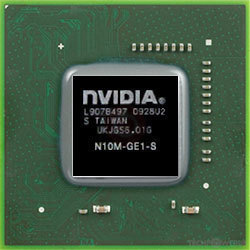
N10M-GE1-S

N10M-GE2-S

G98-630-U2
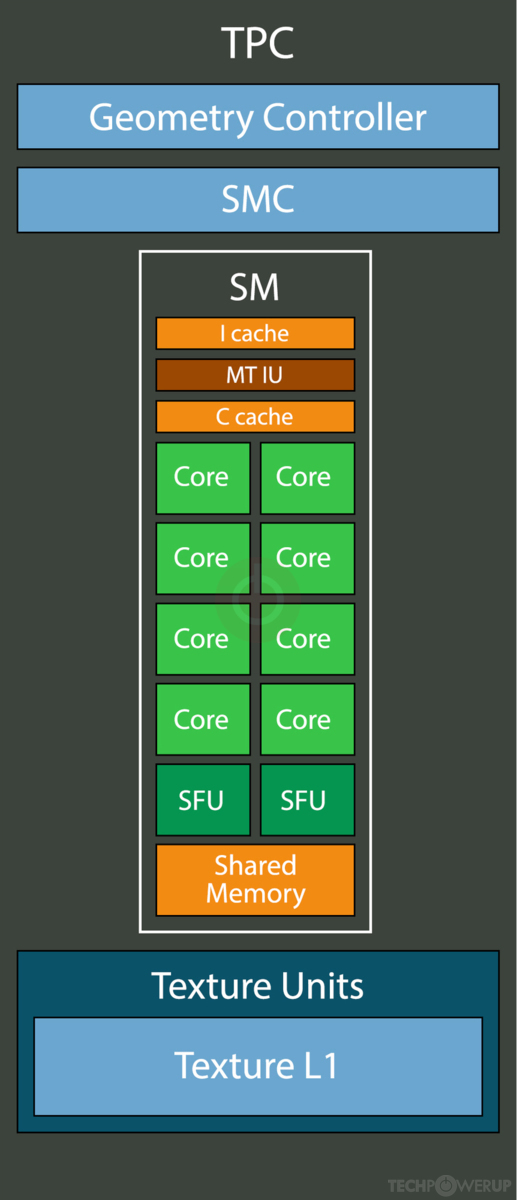
TPC Diagram
NVIDIA's G98S GPU uses the Tesla architecture and is made using a 65 nm production process at UMC. With a die size of 86 mm² and a transistor count of 210 million it is a very small chip. G98S supports DirectX 11.1 (Feature Level 10_0). For GPU compute applications, OpenCL version 1.1 and CUDA 1.1 can be used. It features 8 shading units, 4 texture mapping units and 4 ROPs.
Further reading:
Tesla Architecture Whitepaper 
Graphics Processor
- Released
- Dec 4th, 2007
- GPU Name
- G98S
- Codename
- NV98
- Architecture
- Tesla
- Foundry
- UMC
- Process Size
- 65 nm
- Transistors
- 210 million
- Density
- 2.4M / mm²
- Die Size
- 86 mm²
- Package
- BGA-533
Graphics Features
- DirectX
- 11.1 (10_0)
- OpenGL
- 3.3
- OpenCL
- 1.1
- Vulkan
- N/A
- CUDA
- 1.1
- Shader Model
- 4.0
- WDDM
- 1.2
- PureVideo HD
- VP3
- VDPAU
- Feature Set B
Render Config
- Shading Units
- 8
- TMUs
- 4
- ROPs
- 4
- SM Count
- 1
- SFUs
- 2
- TPCs
- 1
- Tex L1 Cache
- 16 KB per TPC
- L2 Cache
- 16 KB
- Max. TDP
- 40 W
All Tesla GPUs
NVIDIA GPU Architecture History
- 2024 Blackwell
- 2023 Hopper
- 2022-2024 Ada Lovelace
- 2020-2024 Ampere
- 2018-2022 Turing
- 2017-2020 Volta
- 2016-2021 Pascal
- 2014-2019 Maxwell 2.0
- 2014-2017 Maxwell
- 2013-2015 Kepler 2.0
- 2012-2018 Kepler
- 2010-2016 Fermi 2.0
- 2010-2013 VLIW Vec4
- 2010-2016 Fermi
- 2007-2013 Tesla 2.0
- 2006-2010 Tesla
- 2003-2013 Curie
- 2003-2005 Rankine
- 2001-2003 Kelvin
- 1999-2005 Celsius
- 1998-2000 Fahrenheit
Graphics cards using the NVIDIA G98S GPU
| Name | Chip | Memory | Shaders | TMUs | ROPs | GPU Clock | Memory Clock |
|---|---|---|---|---|---|---|---|
| G98-309-U2 | 256 MB | 8 | 4 | 4 | 540 MHz | 400 MHz | |
| 512 MB | 8 | 4 | 4 | 567 MHz | 333 MHz | ||
| G98-409-U2 | 512 MB | 8 | 4 | 4 | 567 MHz | 400 MHz | |
| 256 MB | 8 | 4 | 4 | 540 MHz | 500 MHz | ||
| NB9M-GLM | 256 MB | 8 | 4 | 4 | 580 MHz | 400 MHz | |
| 256 MB | 8 | 4 | 4 | 550 MHz | 700 MHz | ||
| 256 MB | 8 | 4 | 4 | 480 MHz | 700 MHz | ||
| 256 MB | 8 | 4 | 4 | 540 MHz | 695 MHz | ||
| G98-700-U2 | 256 MB | 8 | 4 | 4 | 530 MHz | 700 MHz | |
| NB9M-GS | 256 MB | 8 | 4 | 4 | 580 MHz | 700 MHz | |
| N10M-GE1-S | 512 MB | 8 | 4 | 4 | 640 MHz | 700 MHz | |
| G98-630-U2 | 256 MB | 8 | 4 | 4 | 580 MHz | 400 MHz | |
| G98-630-U2 | 256 MB | 8 | 4 | 4 | 529 MHz | 400 MHz | |
| 256 MB | 8 | 4 | 4 | 540 MHz | 400 MHz | ||
| 256 MB | 8 | 4 | 4 | 540 MHz | 400 MHz | ||
| N10M-GE2-S | 512 MB | 8 | 4 | 4 | 640 MHz | 500 MHz | |
| 256 MB | 8 | 4 | 4 | 540 MHz | 500 MHz | ||
| G98-400-U2 | 512 MB | 8 | 4 | 4 | 567 MHz | 333 MHz |


G98S GPU Notes
| PureVideo HD: VP3 VDPAU: Feature Set B |
Apr 28th, 2024 22:39 EDT
change timezone
Latest GPU Drivers
New Forum Posts
- Your PC ATM (34524)
- AMD Ryzen 9 7950X3D $542 after promo (1)
- Inconsistent cpu-z frequncies (3)
- Is it better for zero RPM PSUs to place the fan on top? (1)
- Share your AIDA 64 cache and memory benchmark here (2920)
- Post your Cinebench R23 Score (2949)
- Size on Disk Excessively Different than Size (10)
- Anyone know if Rufus gets around the SSE4.2 issue with Windows 11 24H2? (45)
- Does charging protection matter? (23)
- What's an inexpensive AIO product line with a strong pump and low price? (86)
Popular Reviews
- Ugreen NASync DXP4800 Plus Review
- HYTE THICC Q60 240 mm AIO Review
- ASUS GeForce RTX 4070 Ti Super TUF Review
- MOONDROP x Crinacle DUSK In-Ear Monitors Review - The Last 5%
- Upcoming Hardware Launches 2023 (Updated Feb 2024)
- Thermalright Phantom Spirit 120 EVO Review
- NVIDIA GeForce RTX 4080 Super Founders Edition Review - Savings of $200
- Logitech G Pro X Superlight 2 Review - Updated with 4000 Hz Tested
- ASUS Radeon RX 7900 GRE TUF OC Review
- FiiO K19 Desktop DAC/Headphone Amplifier Review
Controversial News Posts
- Windows 11 Now Officially Adware as Microsoft Embeds Ads in the Start Menu (139)
- Sony PlayStation 5 Pro Specifications Confirmed, Console Arrives Before Holidays (117)
- NVIDIA Points Intel Raptor Lake CPU Users to Get Help from Intel Amid System Instability Issues (106)
- AMD "Strix Halo" Zen 5 Mobile Processor Pictured: Chiplet-based, Uses 256-bit LPDDR5X (103)
- US Government Wants Nuclear Plants to Offload AI Data Center Expansion (98)
- AMD's RDNA 4 GPUs Could Stick with 18 Gbps GDDR6 Memory (95)
- Windows 10 Security Updates to Cost $61 After 2025, $427 by 2028 (84)
- TechPowerUp Hiring: Reviewers Wanted for Motherboards, Laptops, Gaming Handhelds and Prebuilt Desktops (82)