Report an Error


AMD Radeon R7 370
- Graphics Processor
- Trinidad
- Cores
- 1024
- TMUs
- 64
- ROPs
- 32
- Memory Size
- 2 GB
- Memory Type
- GDDR5
- Bus Width
- 256 bit
GPU
I/O
Top
Recommended Gaming Resolutions:
- 1366x768
- 1600x900
- 1920x1080
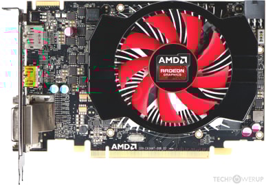
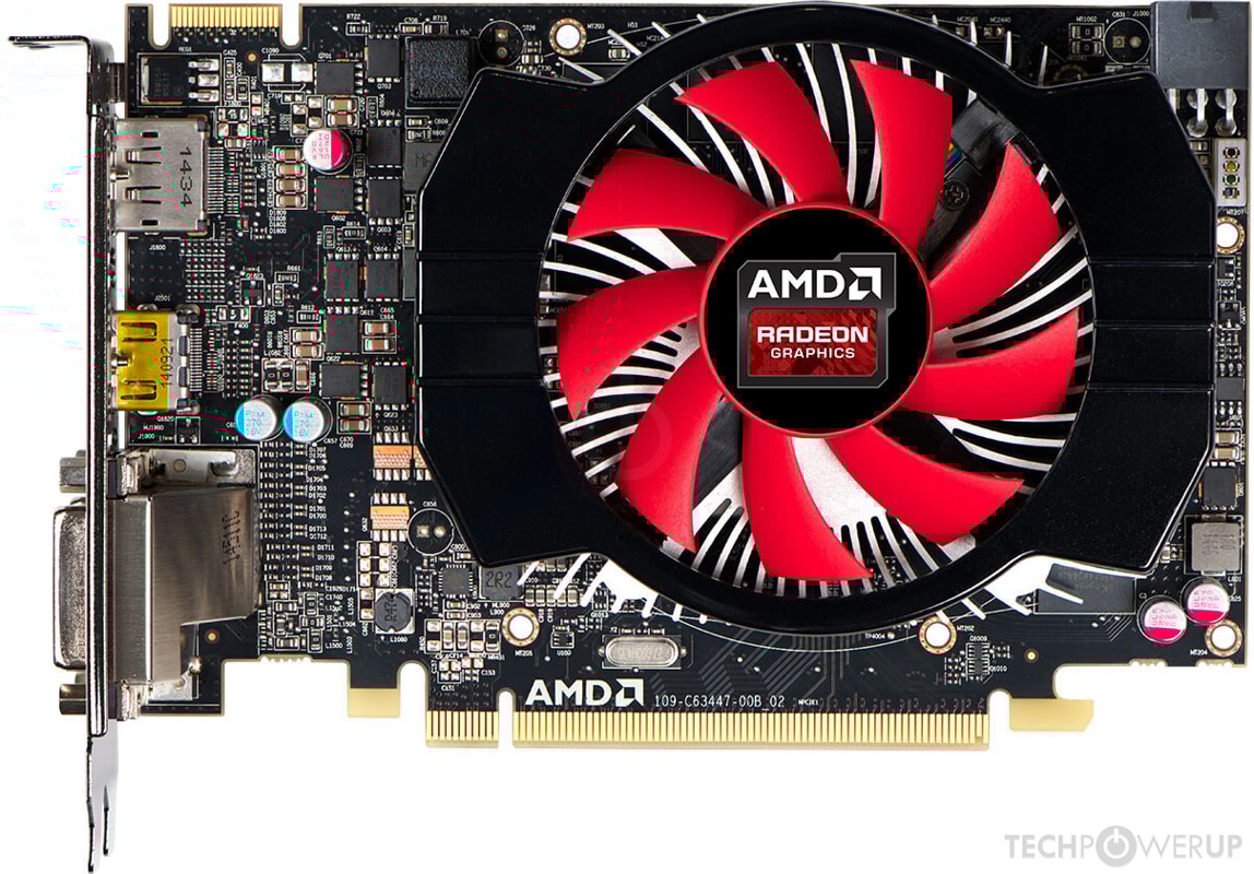
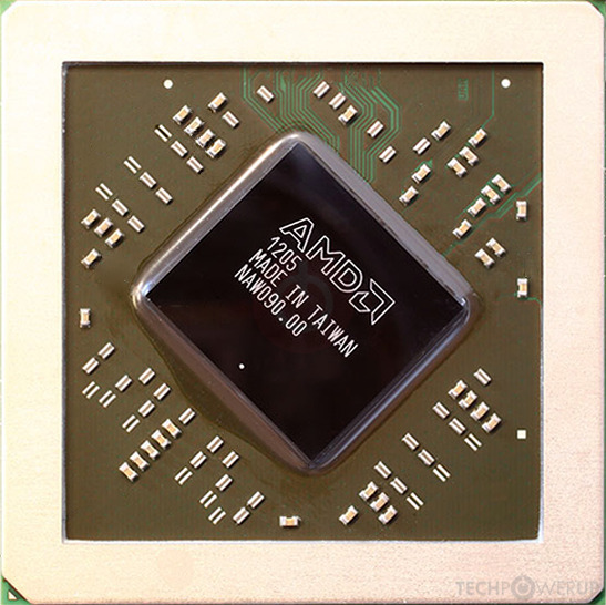
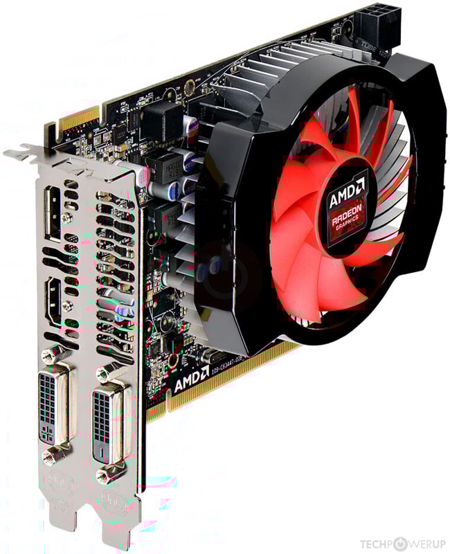
The Radeon R7 370 was a mid-range graphics card by AMD, launched on June 18th, 2015. Built on the 28 nm process, and based on the Trinidad graphics processor, in its Trinidad PRO variant, the card supports DirectX 12. Even though it supports DirectX 12, the feature level is only 11_1, which can be problematic with newer DirectX 12 titles. The Trinidad graphics processor is an average sized chip with a die area of 212 mm² and 2,800 million transistors. Unlike the fully unlocked Radeon R9 370, which uses the same GPU but has all 1280 shaders enabled, AMD has disabled some shading units on the Radeon R7 370 to reach the product's target shader count. It features 1024 shading units, 64 texture mapping units, and 32 ROPs. AMD has paired 2,048 MB GDDR5 memory with the Radeon R7 370, which are connected using a 256-bit memory interface. The GPU is operating at a frequency of 925 MHz, which can be boosted up to 975 MHz, memory is running at 1400 MHz (5.6 Gbps effective).
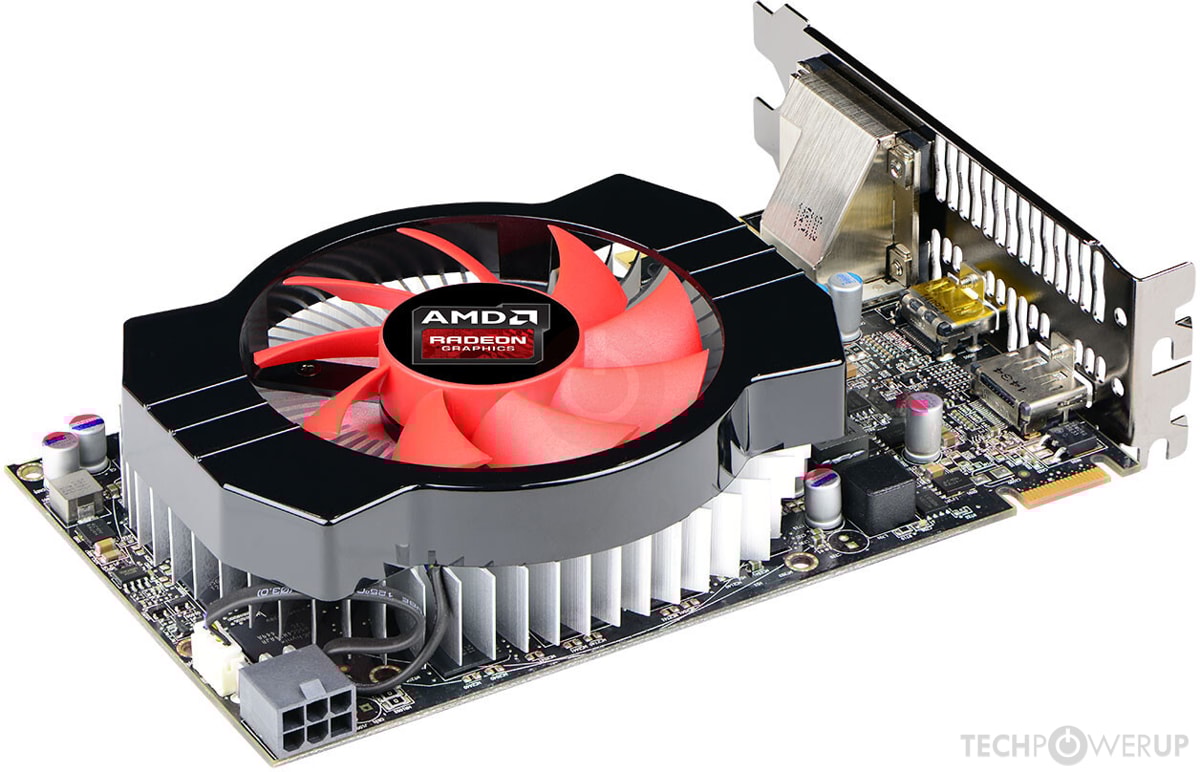
Being a dual-slot card, the AMD Radeon R7 370 draws power from 1x 6-pin power connector, with power draw rated at 110 W maximum. Display outputs include: 2x DVI, 1x HDMI 1.4a, 1x DisplayPort 1.2. Radeon R7 370 is connected to the rest of the system using a PCI-Express 3.0 x16 interface. The card measures 152 mm in length, and features a dual-slot cooling solution. Its price at launch was 149 US Dollars.
Being a dual-slot card, the AMD Radeon R7 370 draws power from 1x 6-pin power connector, with power draw rated at 110 W maximum. Display outputs include: 2x DVI, 1x HDMI 1.4a, 1x DisplayPort 1.2. Radeon R7 370 is connected to the rest of the system using a PCI-Express 3.0 x16 interface. The card measures 152 mm in length, and features a dual-slot cooling solution. Its price at launch was 149 US Dollars.
Graphics Processor
Graphics Card
- Release Date
- Jun 18th, 2015
- Generation
-
Pirate Islands
(R7 300)
- Predecessor
- Volcanic Islands
- Successor
- Arctic Islands
- Production
- End-of-life
- Launch Price
- 149 USD
- Bus Interface
- PCIe 3.0 x16
- Reviews
- 21 in our database
Relative Performance
Based on TPU review data: "Performance Summary" at 1920x1080, 4K for RTX 3080 and faster.
Clock Speeds
- Base Clock
- 925 MHz
- Boost Clock
- 975 MHz
- Memory Clock
-
1400 MHz
5.6 Gbps effective
Memory
- Memory Size
- 2 GB
- Memory Type
- GDDR5
- Memory Bus
- 256 bit
- Bandwidth
- 179.2 GB/s
Render Config
- Shading Units
- 1024
- TMUs
- 64
- ROPs
- 32
- Compute Units
- 16
- L1 Cache
- 16 KB (per CU)
- L2 Cache
- 512 KB
Theoretical Performance
- Pixel Rate
- 31.20 GPixel/s
- Texture Rate
- 62.40 GTexel/s
- FP32 (float)
- 1.997 TFLOPS
- FP64 (double)
- 124.8 GFLOPS (1:16)
Board Design
- Slot Width
- Dual-slot
- Length
- 152 mm
6 inches
- TDP
- 110 W
- Suggested PSU
- 300 W
- Outputs
- 2x DVI
1x HDMI 1.4a
1x DisplayPort 1.2
- Power Connectors
- 1x 6-pin
- Board Number
- C631,
109-C63447-00B_02
Graphics Features
- DirectX
- 12 (11_1)
- OpenGL
- 4.6
- OpenCL
- 2.1 (1.2)
- Vulkan
- 1.2.170
- Shader Model
- 6.5 (5.1)
Trinidad GPU Notes
| Generation: Southern Islands Desktop Variant: Pitcairn / Curacao Mobile Variant: Wimbledon / Neptune Graphics/Compute: GFX6 (gfx601) Display Core Engine: 6.0 Unified Video Decoder: 4.0 Video Compression Engine: 1.0 CLRX: GCN 1.0 Latest Drivers: Windows XP / 8: Catalyst Software Suite 14.4 Windows Vista : Catalyst Software Suite 13.12 Windows 7: 32-bit: Radeon Software: Adrenalin Edition 18.9.3 64-bit: AMD Software: Adrenalin Edition 22.6.1 Windows 8.1: 32-bit: Radeon Software: Crimson ReLive Edition 16.12.2 / 17.1.2 64-bit: Radeon Software: Crimson ReLive Edition 17.4.4 / 17.7.1 Windows 10: 32-bit: Radeon Software: Adrenalin Edition 18.9.3 64-bit: AMD Software: Adrenalin Edition 22.6.1 |
Retail boards based on this design (21)
| Name | GPU Clock | Boost Clock | Memory Clock | Other Changes |
|---|---|---|---|---|
| 925 MHz | 975 MHz | 1400 MHz | 228 mm/9 inches | |
| 925 MHz | 975 MHz | 1400 MHz | 4 GB, 214 mm/8.4 inches | |
| 925 MHz | 1050 MHz | 1400 MHz | 228 mm/9 inches | |
| 925 MHz | 1050 MHz | 1400 MHz | 4 GB, 214 mm/8.4 inches | |
| 965 MHz | 1015 MHz | 1400 MHz | 194 mm/7.6 inches | |
| 975 MHz | 1000 MHz | 1400 MHz | 270 mm/10.6 inches | |
| 970 MHz | 1020 MHz | 1400 MHz | 255 mm/10 inches | |
| 980 MHz | 1030 MHz | 1400 MHz | 258 mm/10.2 inches | |
| 980 MHz | 1030 MHz | 1400 MHz | 4 GB, 258 mm/10.2 inches | |
| 970 MHz | 1020 MHz | 1400 MHz | 255 mm/10 inches | |
| 935 MHz | 985 MHz | 1425 MHz | 220 mm/8.7 inches | |
| 985 MHz | 1035 MHz | 1400 MHz | 228 mm/9 inches | |
| 925 MHz | 985 MHz | 1400 MHz | 170 mm/6.7 inches | |
| 925 MHz | 985 MHz | 1400 MHz | 4 GB, 211 mm/8.3 inches | |
| 925 MHz | 1075 MHz | 1450 MHz | 4 GB, 264 mm/10.4 inches | |
| 925 MHz | 995 MHz | 1400 MHz | 221 mm/8.7 inches | |
| 925 MHz | 975 MHz | 1400 MHz | 4 GB | |
| 925 MHz | 995 MHz | 1400 MHz | 234 mm/9.2 inches | |
| 925 MHz | 995 MHz | 1400 MHz | 4 GB, 234 mm/9.2 inches | |
| 1000 MHz | 1050 MHz | 1400 MHz | 221 mm/8.7 inches | |
| 925 MHz | 1040 MHz | 1450 MHz | 234 mm/9.2 inches |


Jul 31st, 2025 16:14 CDT
change timezone
Latest GPU Drivers
New Forum Posts
- PSUs exploding during water loop test. (37)
- AI Job Losses: let's count the losses up, total losses to AI so far 94,000 and counting (95)
- Are UPS lithium LiFePO4 batteries finally as cheap as lead-acid? (58)
- I just bought an RX570 4Gb (20)
- 3D Printer Club (577)
- Choosing the right motherboard (21)
- Once more EDP OTHER (1)
- Suggestions for UI improvement (3)
- Image navigation in reviews/articles etc. (5)
- Free Games Thread (4823)
Popular Reviews
- MSI Claw 8 AI+ A2VM Review
- Lenovo Legion 5i (15IRX10) Review - Feature-Rich and Wallet Friendly
- Herman Miller Logitech G Embody Review - No Pain, No Gain
- ASUS ROG Crosshair X870E Apex Review
- Orbital Pathfinder Review
- Lian Li O11 Dynamic Mini V2 Review
- Upcoming Hardware Launches 2025 (Updated May 2025)
- Noctua NF-A12x25 G2 PWM Fan Review
- Sapphire Radeon RX 9060 XT Pulse OC 16 GB Review - An Excellent Choice
- AMD Ryzen 7 9800X3D Review - The Best Gaming Processor
TPU on YouTube
Controversial News Posts
- AMD's Upcoming UDNA / RDNA 5 GPU Could Feature 96 CUs and 384-bit Memory Bus (137)
- AMD Radeon RX 9070 XT Gains 9% Performance at 1440p with Latest Driver, Beats RTX 5070 Ti (131)
- Intel "Nova Lake-S" Core Ultra 3, Ultra 5, Ultra 7, and Ultra 9 Core Configurations Surface (110)
- DDR6 Memory Arrives in 2027 with 8,800-17,600 MT/s Speeds (102)
- NVIDIA to Debut GeForce RTX 50-series SUPER GPUs by Christmas (98)
- AMD Sampling Next-Gen Ryzen Desktop "Medusa Ridge," Sees Incremental IPC Upgrade, New cIOD (97)
- Intel CEO Confirms SMT To Return to Future CPUs (95)
- NVIDIA Becomes First Company Ever to Hit $4 Trillion Market-Cap (94)