Report an Error


NVIDIA GeForce GTX 480
- Graphics Processor
- GF100
- Cores
- 480
- TMUs
- 60
- ROPs
- 48
- Memory Size
- 1536 MB
- Memory Type
- GDDR5
- Bus Width
- 384 bit


GPU
I/O

Bottom

PCB Front

PCB Back
Recommended Gaming Resolutions:
- 1366x768
- 1600x900
- 1920x1080
The GeForce GTX 480 was a high-end graphics card by NVIDIA, launched on March 26th, 2010. Built on the 40 nm process, and based on the GF100 graphics processor, in its GF100-375-A3 variant, the card supports DirectX 12. Even though it supports DirectX 12, the feature level is only 11_0, which can be problematic with newer DirectX 12 titles. The GF100 graphics processor is a large chip with a die area of 529 mm² and 3,100 million transistors. Unlike the fully unlocked GeForce GTX 480 Core 512, which uses the same GPU but has all 512 shaders enabled, NVIDIA has disabled some shading units on the GeForce GTX 480 to reach the product's target shader count. It features 480 shading units, 60 texture mapping units, and 48 ROPs. NVIDIA has paired 1,536 MB GDDR5 memory with the GeForce GTX 480, which are connected using a 384-bit memory interface. The GPU is operating at a frequency of 701 MHz, memory is running at 924 MHz (3.7 Gbps effective).
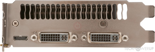
Being a dual-slot card, the NVIDIA GeForce GTX 480 draws power from 1x 6-pin + 1x 8-pin power connector, with power draw rated at 250 W maximum. Display outputs include: 2x DVI, 1x mini-HDMI 1.3a. GeForce GTX 480 is connected to the rest of the system using a PCI-Express 2.0 x16 interface. The card measures 267 mm in length, and features a dual-slot cooling solution. Its price at launch was 499 US Dollars.
Being a dual-slot card, the NVIDIA GeForce GTX 480 draws power from 1x 6-pin + 1x 8-pin power connector, with power draw rated at 250 W maximum. Display outputs include: 2x DVI, 1x mini-HDMI 1.3a. GeForce GTX 480 is connected to the rest of the system using a PCI-Express 2.0 x16 interface. The card measures 267 mm in length, and features a dual-slot cooling solution. Its price at launch was 499 US Dollars.
Graphics Processor
Graphics Card
- Release Date
- Mar 26th, 2010
- Generation
- GeForce 400
- Predecessor
- GeForce 200
- Successor
- GeForce 500
- Production
- End-of-life
- Launch Price
- 499 USD
- Bus Interface
- PCIe 2.0 x16
- Reviews
- 84 in our database
Relative Performance
Based on TPU review data: "Performance Summary" at 1920x1080, 4K for RTX 3080 and faster.
Clock Speeds
- GPU Clock
- 701 MHz
- Shader Clock
- 1401 MHz
- Memory Clock
-
924 MHz
3.7 Gbps effective
Memory
- Memory Size
- 1536 MB
- Memory Type
- GDDR5
- Memory Bus
- 384 bit
- Bandwidth
- 177.4 GB/s
Render Config
- Shading Units
- 480
- TMUs
- 60
- ROPs
- 48
- SM Count
- 15
- L1 Cache
- 64 KB (per SM)
- L2 Cache
- 768 KB
Theoretical Performance
- Pixel Rate
- 21.03 GPixel/s
- Texture Rate
- 42.06 GTexel/s
- FP32 (float)
- 1,345.0 GFLOPS
- FP64 (double)
- 168.1 GFLOPS (1:8)
Board Design
- Slot Width
- Dual-slot
- Length
- 267 mm
10.5 inches
- TDP
- 250 W
- Suggested PSU
- 600 W
- Outputs
- 2x DVI
1x mini-HDMI 1.3a
- Power Connectors
- 1x 6-pin + 1x 8-pin
- Board Number
- P1022 SKU 0000
Graphics Features
- DirectX
- 12 (11_0)
- OpenGL
- 4.6
- OpenCL
- 1.1
- Vulkan
- N/A
- CUDA
- 2.0
- Shader Model
- 5.1
GF100 GPU Notes
| PureVideo HD: VP4 VDPAU: Feature Set C GF100 has 4 GPCs each capable of 8 pixels per clock. This limits complete GPU to 32 pixels per clock and because of that it can't feed all 48 ROPs when they all require data at the same time. Additional ROPs however can be used for MSAA (because it doesn't require additional data from rasterizers, while giving more work to ROPs.) Latest Drivers: Windows 2000: Quadro Release 261.19 Windows XP / Server 2003 x64: GeForce Release 368.81 Quadro Release R319 U2 (321.01) Tesla Release 340.62 / R319 U2 (321.01) Windows Vista: GeForce Release 365.19 Quadro Release R346 U7 (348.40) Tesla Release 340.84 Windows 7 / 8 / 8.1 / 10 (x32 / x64): GeForce Release 391.35 Quadro Release R375 U11 (377.83) Tesla Release 340.84 / 412.29 |
Retail boards based on this design (17)
| Name | GPU Clock | Memory Clock | Other Changes |
|---|---|---|---|
| 701 MHz | 924 MHz | ||
| 701 MHz | 924 MHz | ||
| 701 MHz | 924 MHz | ||
| 752 MHz | 950 MHz | Single-slot, 2x DVI 1x HDMI | |
| 726 MHz | 950 MHz | ||
| 726 MHz | 950 MHz | ||
| 701 MHz | 924 MHz | ||
| 821 MHz | 950 MHz | 279 mm/11 inches | |
| 760 MHz | 950 MHz | ||
| 701 MHz | 924 MHz | ||
| 701 MHz | 924 MHz | ||
| 701 MHz | 924 MHz | ||
| 750 MHz | 1000 MHz | 305 mm/12 inches, 2x DVI 1x HDMI 1x DisplayPort | |
| 701 MHz | 924 MHz | 265 mm/10.4 inches | |
| 701 MHz | 924 MHz | ||
| 701 MHz | 924 MHz | ||
| 756 MHz | 950 MHz |


Jul 28th, 2025 18:23 CDT
change timezone
Latest GPU Drivers
New Forum Posts
- Inno3D iChiLL (1)
- Which Linux flavor? (76)
- What are you playing? (24022)
- Spoiler Alert........this car is fast. (254)
- Warning about DOCP (22)
- Kindly help me to complete my new PC build... (18)
- What's your latest tech purchase? (24382)
- Future-Proof Build for Music Production and Work - Will these parts work well together? (18)
- What antivirus do you use? (35)
- 2022-X58/1366 PIN Motherboards NVME M.2 SSD BIOS MOD Collection (947)
Popular Reviews
- Herman Miller Logitech G Embody Review - No Pain, No Gain
- Lian Li O11 Dynamic Mini V2 Review
- AQIRYS Sirius Pro Review
- Noctua NF-A12x25 G2 PWM Fan Review
- Upcoming Hardware Launches 2025 (Updated May 2025)
- VAXEE XE V2 Wireless Review
- UPERFECT UMax 24 Review
- DDR5 Memory Performance Scaling with AMD Zen 5
- Sharkoon OfficePal C10 Review - Affordable and Decent
- AMD Ryzen 7 9800X3D Review - The Best Gaming Processor
TPU on YouTube
Controversial News Posts
- AMD's Upcoming UDNA / RDNA 5 GPU Could Feature 96 CUs and 384-bit Memory Bus (134)
- AMD Radeon RX 9070 XT Gains 9% Performance at 1440p with Latest Driver, Beats RTX 5070 Ti (131)
- NVIDIA GeForce RTX 5080 SUPER Could Feature 24 GB Memory, Increased Power Limits (115)
- Intel "Nova Lake-S" Core Ultra 3, Ultra 5, Ultra 7, and Ultra 9 Core Configurations Surface (108)
- NVIDIA DLSS Transformer Cuts VRAM Usage by 20% (100)
- DDR6 Memory Arrives in 2027 with 8,800-17,600 MT/s Speeds (99)
- AMD Sampling Next-Gen Ryzen Desktop "Medusa Ridge," Sees Incremental IPC Upgrade, New cIOD (97)
- Intel CEO Confirms SMT To Return to Future CPUs (95)