News Posts matching #12 nm

Return to Keyword Browsing

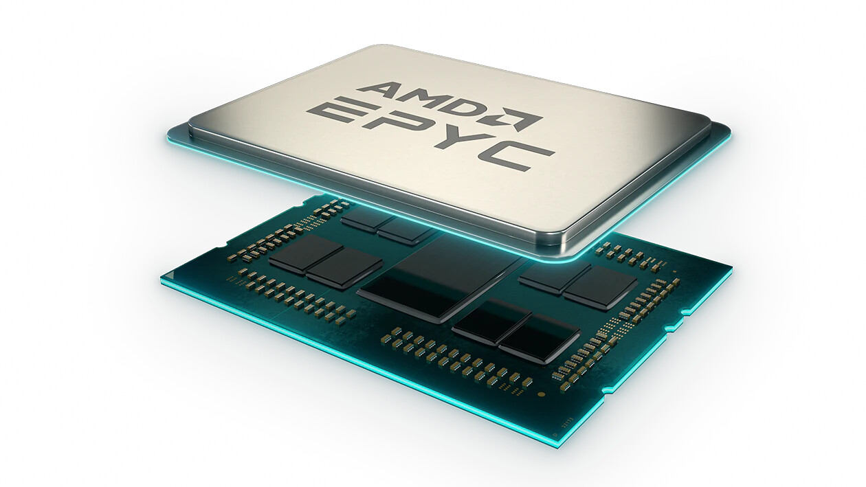
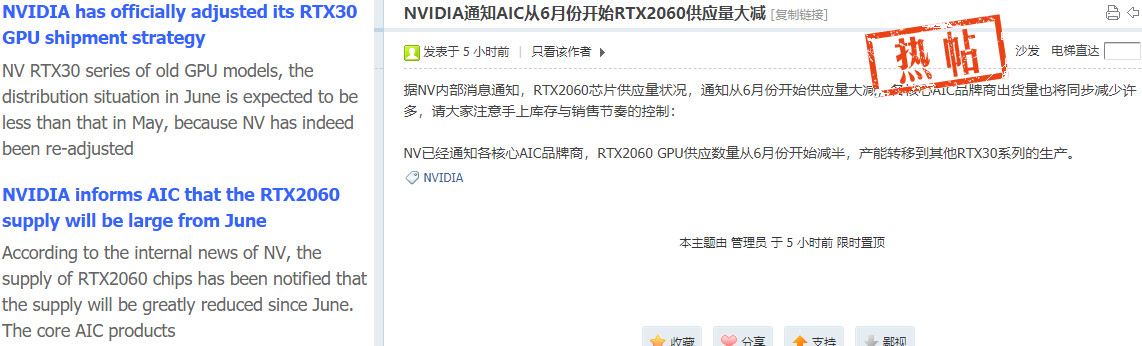
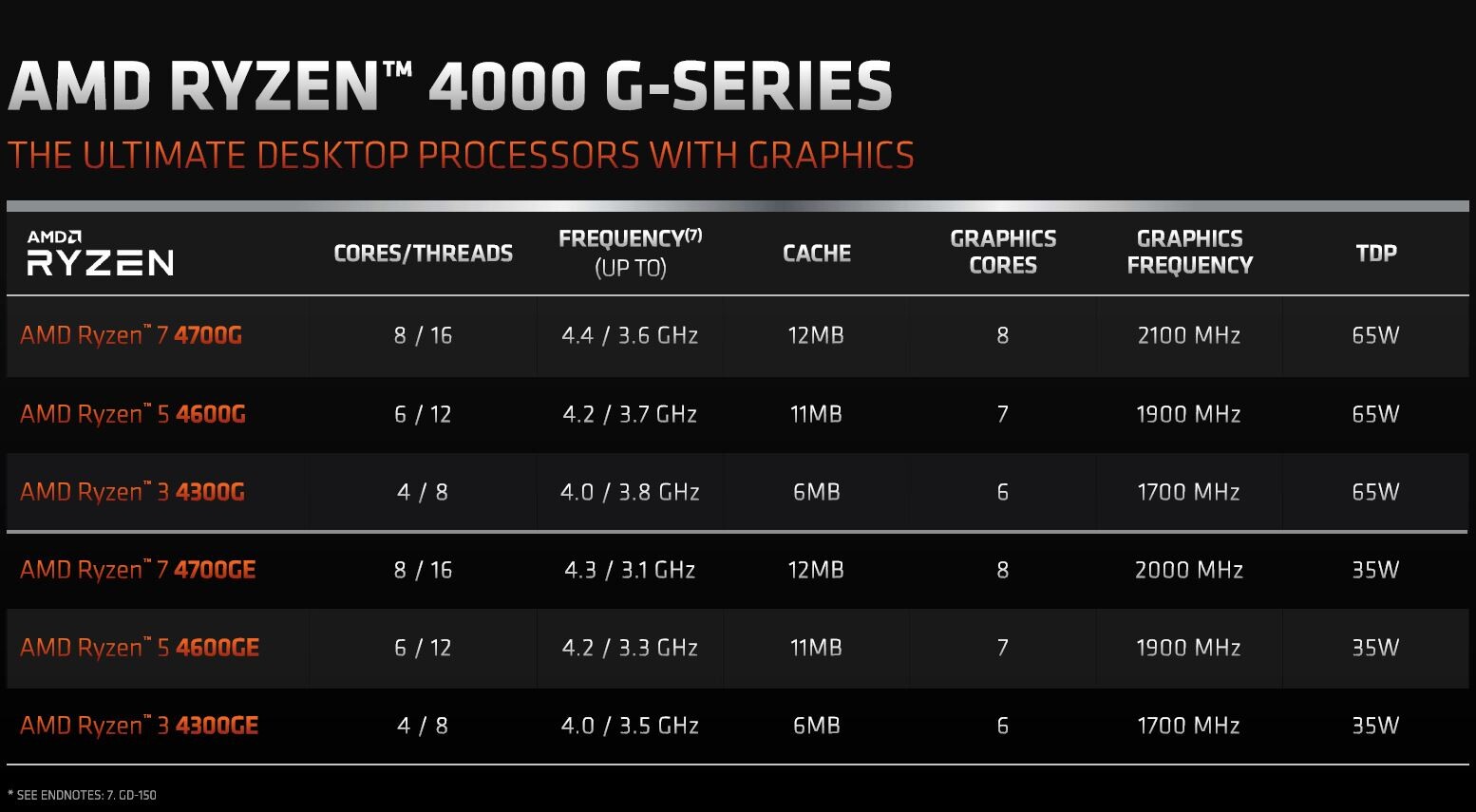
AMD and GlobalFoundries Renew Wafer Supply Agreement

AMD in its 8-K filing with the SEC, disclosed that it has updated its wafer supply agreement (WSA) with GlobalFoundries. Under the latest agreement, AMD commits to buy $2.1 billion worth wafers from GlobalFoundries between 2022 and 2025. The previous version of the WSA saw commitments up to 2024, and wafers worth $1.6 billion. The update hence adds another year and $500 million worth supply.

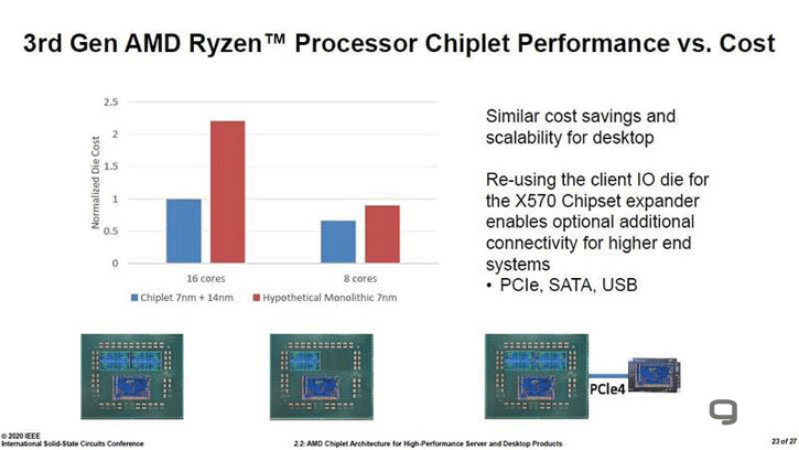
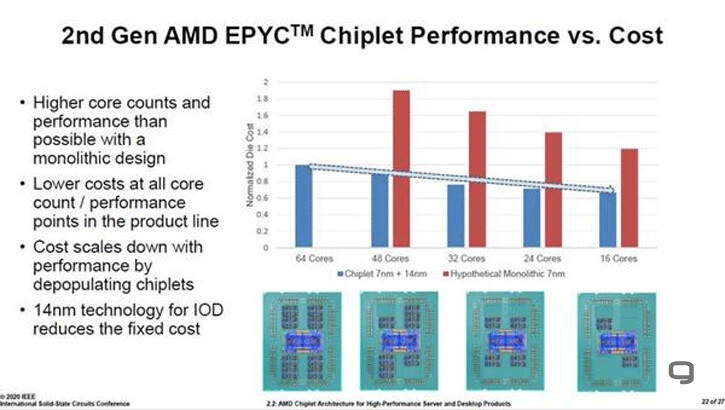
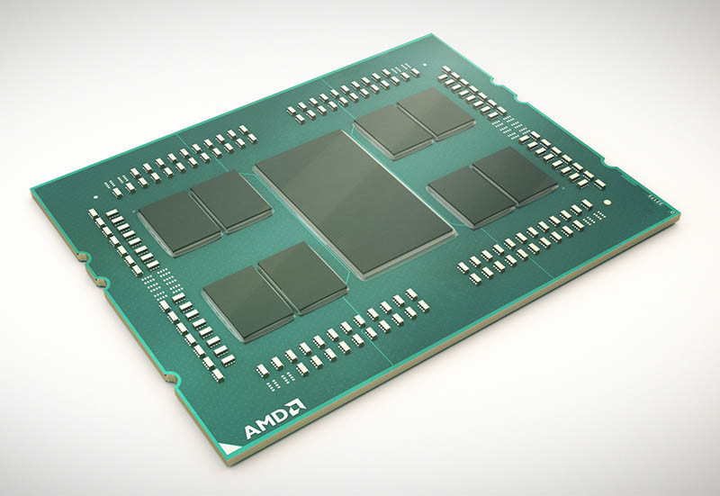
AMD currently sources 12 nm and 14 nm wafers from GlobalFoundries, which go into making cIOD and sIOD components in its processors, and motherboard chipsets. The move to extend the WSA indicates that the company may continue to use 12 nm-class I/O dies in its processors for the foreseeable future. It will be very interesting to see if 12 nm-class I/O dies make it to next-generation products such as "Genoa" and "Rapael," which integrate the latest IP blocks such as PCI-Express Gen 5 root-complexes, DDR5 memory controllers, and 3rd Gen Infinity Fabric. Processors with 12 nm I/O dies, such as "Milan" and "Vermeer" could be retired only by 2023-24, as AMD will use 2022 to spread across its next-gen product launches.

Gigabyte Registers Four NVIDIA GeForce RTX 2060 12 GB Graphics Cards With the EEC

The on-again, off-again relationship between NVIDIA and its Turing-based RTX 2060 graphics seems to be heading towards a new tipping point. As previously reported, NVIDIA is expected to be preparing another release cycle for its RTX 2060 graphics card - this time, paired with an as puzzling as it is gargantuan (for its shader performance) 12 GB of GDDR6 memory. Gigabyte has given us yet another tip at the card's expected launch by the end of this year or early 2022 by registering four different card models with the EEC (Eurasian Economic Commission). Gigabyte's four registered cards carry the model numbers GV-N2060OC-12GD, GV-N2060D6-12GD, GV-N2060WF2OC-12GD, and GV-N2060WF2-12GD. Do however remember that not all registered graphics cards actually make it to market.

NVIDIA's revival of the RTX 2060 towards the current market conditions speaks in volumes. While NVIDIA is producing as many 8 nm cards as it can with foundry partner Samsung, the current state of the graphics card pricing market leaves no doubts as to how successfully NVIDIA has been able to cope with both the logistics and materials constraints currently experienced by the semiconductor market. The 12 nm manufacturing process certainly has more available capacity than Samsung's 8 nm; at the same time, the RTX 2060's mining capabilities have been overtaken by graphics cards from the Ampere family, meaning that miners most likely will not look at these as viable options for mining, thus improving availability for consumers as well. If the card does keep close to its expected $300 price-point upon release, of course.

MediaTek Announces Filogic Connectivity Family with New Filogic 830 and Filogic 630 Wi-Fi 6/6E Chips

MediaTek today unveiled its new Filogic connectivity family with the introduction of the Filogic 830 Wi-Fi 6/6E system-on-chip (SoC) and Filogic 630 Wi-Fi 6E network interface card (NIC) solutions. MediaTek's new Filogic series of high-performance Wi-Fi 6/6E chipsets provide reliable connectivity, high computation capabilities and a rich set of features in highly integrated, power-efficient designs.

"The MediaTek Filogic series ushers in a new era of smart Wi-Fi solutions with extreme speeds, low latency and superb power efficiency for seamless, always connected experiences," said Alan Hsu, Corporate Vice President & General Manager, Intelligent Connectivity at MediaTek. "These new chipsets provide best-in-class features with highly integrated designs for the next generation of premium broadband, enterprise and retail Wi-Fi solutions."

Phison is Enabling Custom PCIe Gen 5 SSDs to Ship in 2022, New E26-series Processor

Phison Electronics Corp., a global leader in NAND flash controller integrated circuits and storage solutions, today announced its technology development of PCIe Gen 5 customizable SSD solutions for Enterprise and Client SSDs. Phison customers from Hyperscale Cloud Data Centers to PC Gaming demand the fastest performance motherboards and SSD storage devices. Their business models require that they transition to the newest technologies when they first become available, usually well before the rest of the software and hardware ecosystem has been established.

Phison is enabling our valued customers with PCIe Gen 5 SSD platforms that may be customized to perform optimally in their applications. Customers who are early adopters of PCIe Gen 5 SSDs will benefit from superior specifications and first to market leadership revenue. The data rate specification for PCIe Gen 5 at 32 Gb/s is twice the lane speed of PCIe Gen 4 at 16 Gb/s, enabling either double the overall performance, or offering similar performance, but using half as many lanes as PCIe Gen 4.

Foundry Revenue for 2Q21 Reaches Historical High Once Again with 6% QoQ Growth Thanks to Increased ASP and Persistent Demand, Says TrendForce

The panic buying of chips persisted in 2Q21 owing to factors such as post-pandemic demand, industry-wide shift to 5G telecom technology, geopolitical tensions, and chronic chip shortages, according to TrendForce's latest investigations. Chip demand from ODMs/OEMs remained high, as they were unable to meet shipment targets for various end-products due to the shortage of foundry capacities. In addition, wafers inputted in 1Q21 underwent a price hike and were subsequently outputted in 2Q21. Foundry revenue for the quarter reached US$24.407 billion, representing a 6.2% QoQ increase and yet another record high for the eighth consecutive quarter since 3Q19.

NVIDIA Reportedly Cutting RTX 2060 Fabrication to Focus on RTX 30-series

NVIDIA is reported to be cutting down on production of its highly popular RTX 2060 graphics card, in a bid to increase production of the RTX 30-series graphics cards that still elude most consumers looking to get one on their gaming rig. The decision may be motivated by increased margins on RTX 30-series products, as well as by the continuing component shortage in the industry, with even GDDR6 becoming a limiting factor to production capability.

While one might consider this a strange move at face value (Turing is manufactured on TSMC's 12 nm node, whilst Ampere is manufactured on Samsung's 8 nm), the fact of the matter is that there are a multitude of components required for GPUs besides the graphics processing silicon proper; and NVIDIA essentially sells ready-to-produce kits to AICs (Add-in-Card Partners) which already include all the required components, circuitry, and GPU slice to put together. And since supply on most components and even simple logic is currently strained, every component in an RTX 2060-allocated kit could be eating into final production capacity for the RTX 30-series graphics cards - hence the decision to curb the attempt to satiate pent-up demand with a last-generation graphics card and instead focusing on current-gen hardware.

AMD and GlobalFoundries Wafer Supply Agreement Now Non-Exclusive, Paves Way for 7nm sIOD

AMD in a filing with the U.S. Securities and Exchange Commission (SEC), revealed that its wafer supply agreement with GlobalFoundries has been amended. Under the new terms, AMD places orders for wafers from GlobalFoundries up to 2024, with purchase targets set for each year leading up to 2024. Beyond meeting these targets, AMD is free from all other exclusivity commitments. The agreement was previously amended in January 2019, setting annual purchase targets for 2019, 2020, and 2021, while beginning a de-coupling between AMD and GlobalFoundries. This enabled the company to source 7 nm (or smaller) chips, such as CCDs and GPUs, from other foundries, such as TSMC, while keeping GlobalFoundries exclusive for 12 nm (or larger) nodes.

The updated wafer supply agreement unlocks many possibilities for AMD. For starters, it can finally build a next-generation sIOD (server I/O die) on a more efficient node than GlobalFoundries 12LP, such as TSMC 7 nm. This transition to 7 nm will be needed as the next-gen "Genoa" EPYC processor could feature future I/O standards such as DDR5 memory and PCI-Express Gen 5, and the switching fabric for these could be too power-hungry on 12 nm. The "Zen 4" CPU core complex dies (CCDs) of "Genoa" are expected to be built on TSMC 5 nm.

Phison Delivers Fastest PCIe Gen 4x4 NVMe SSD Controller, the E18 Series

Phison Electronics, the industry leader in flash controller technology, is delivering the storage industry's fastest PCIe Gen 4x4 NVMe SSD solution, its second generation PS5018-E18 (E18) PCIe 4.0 controller. The E18 succeeds the PS5016-E16 released in late 2019.

Phison designed the new E18 from the ground up on the efficient TSMC 12 nm process node. This provides SSD manufacturers with a state-of-the-art controller solution in an increasingly competitive field. The controller utilizes Phison's proprietary CoXProcessor 2.0 technology, an innovative SSD architecture that enables E18 to deliver exceptional performance and power efficiency. Phison architecture is also primed for AI-assisted storage, where its distributed architecture uses many small cores to perform the workload in parallel. The E18 is ideal for gamers, content creators, and computing enthusiasts, which demand the best experience. This ultra-low latency is possible only with NVMe SSDs.

AMD Ryzen 3000C-series Processors Based on Existing "Zen+" IP, Heavy TDP Optimization

AMD earlier today announced its Ryzen 3000C-series processors targeted at Chromebooks, a segment where the company feels it can bring more to the table than Intel's entry-level Celeron, Pentium Silver, and Pentium Gold mobile processors. Responding to a questionnaire by TechPowerUp, AMD revealed a handful details about these processors. The Ryzen 3000C-series processors are based on the 12 nm "Picasso" silicon, while the Athlon Gold and Athlon Silver parts are based on 14 nm. The "Picasso" based parts combine up to 4 "Zen+" CPU cores, with an iGPU based on the "Vega" graphics architecture, with up to 10 NGCUs. AMD has optimized all SKUs for a 15 W TDP target.

Responding to a question on storage specification or possible collaboration with MediaTek on WLAN controllers, AMD responded that it wishes a diverse hardware ecosystem for its OEM partners, without getting into specifics. There was no denial on the MediaTek bit. The Ryzen 7 3700C practically maxes out the "Picasso" silicon within the 15 W TDP envelope, which got us wondering if AMD has its eyes on the premium Chromebook segment, possibly even Google's first-party Chromebook Pixel brand. To this company responded that while the 3700C has a solid feature-set for premium Chromebooks, there are no first-party Pixel products on the anvil. AMD has just entered the market, and possibly wants to make a dent on the bulk of the Chromebook market first.

TSMC Details 3nm N3, 5nm N5, and 3DFabric Technology

TSMC on Monday kicked off a virtual tech symposium, where it announced its new 12 nm N12e node for IoT edge devices, announced the new 3DFabric Technology, and detailed progress on its upcoming 5 nm N5 and 3 nm N3 silicon fabrication nodes. The company maintains that the N5 (5 nm) node offers the benefits of a full node uplift over its current-gen N7 (7 nm), which recently clocked over 1 billion chips shipped. The N5 node incorporates EUV lithography more extensively than N6/N7+, and in comparison to N7 offers 30% better power at the same performance, 15% more performance at the same power, and an 80% increase in logic density. The company has commenced high-volume manufacturing on this node.

2021 will see the introduction and ramp-up of the N5P node, an enhancement of the 5 nm N5 node, offering a 10% improvement in power at the same performance, or 5% increase in performance at the same power. A nodelet of the N5 family of nodes, called N4, could see risk production in Q4 2021. The N4 node is advertised as "4 nm," although the company didn't get into its iso-power/iso-performance specifics over the N5 node. The next major node for TSMC will be the 3 nm N3 node, with massive 25%-30% improvement in power at the same performance, or 10%-15% improvement in performance at same power, compared to N5. It also offers a 70% logic density gain over N5. 3DFabric technology is a new umbrella term for TSMC's CoWoS (chip on wafer on substrate), CoW (chip on wafer), and WoW (wafer on wafer) 3-D packaging innovations, with which it plans to offer packaging innovations that compete with Intel's various new 3D chip packaging technologies on the anvil.

TSMC Announces the N12e Enhanced 12nm FF Node for 5G and IoT Edge Devices

TSMC on Monday announced the N12e silicon fabrication node. An enhancement of its 12 nm FinFET node, N12e is designed for value 5G application processors, MODEMs, and IoT edge devices, such as true-wireless earbuds, smartwatch processors, wearables, VR HMDs, entry-level and mainstream SoCs, etc. The node has been derived from the company's 12FFC+_ULL node, and fits into the 12-16 nm class of nodes. It's intended to succeed the company's 22ULL node (in terms of pricing), offering a 76% increase in logic density, 49% increase in clock speed at a given power, 55% improvement in power draw at a given speed, 50% reduction in SRAM leakage current, and low Vdd, with support for logic voltages as low as 0.4 V. That last bit in particular should make the node suitable for tiny, battery-powered devices such as wearables.

DigiTimes Research: China 14th 5-year Plan to see IC Foundry Capacity Expand 40%

China's upcoming 14th five-year plan (2021-2025) will continue to highlight technology and capacity upgrades as the core of its semiconductor self-sufficiency strategy, with foundry capacity projected to expand 40% from the preceding plan and fabrication process expected to advance to 7 nm, according to Digitimes Research.

Bolstered by national policies in the 13th five-year plan, China's IC manufacturing industry is expected to see combined revenues double to CNY240 billion (US$34.28 million) in 2020 from 2016, and may also move 12 nm to production by the end of the year after having volume produced 14 nm process.

AMD Announces Renoir for Desktop: Ryzen 4000G, PRO 4000G, and Athlon PRO 3000G

AMD today announced its 4th Generation Ryzen 4000G and Ryzen PRO 4000G desktop processors for pre-built OEM desktops. The company also expanded its entry-level Athlon 3000G series and debuted the Athlon PRO 3000G series. The Ryzen 4000G and PRO 4000G mark the Socket AM4 desktop debut of the 7 nm "Renoir" silicon, which combines up to 8 CPU cores based on the "Zen 2" microarchitecture, with a Radeon Vega 8 iGPU. These processors benefit from the 65 W TDP and increased power limits of the desktop platform to dial up CPU- and iGPU engine clock speeds significantly over the Ryzen 4000U and 4000H mobile processors based on the same silicon. The new Athlon 3000G-series and Athlon PRO 3000G-series parts are based on a 12 nm die that has "Zen+" CPU cores.

All of the processor models announced today are OEM-only, meaning that you'll only find them on pre-built consumer- and commercial desktops by the likes of HP, Lenovo, Dell, etc. Not even the system-integrator (SI) channel (eg: Maingear, Origin PC, etc.,) gets these chips. OEMs will pair these processors with motherboards based on the AMD B550 chipset, although the chips are compatible with the X570 chipset, too. The Ryzen PRO 4000G processors are targeted at commercial desktops that are part of large business environments, and launches along with the new AMD PRO565 chipset. Since they are OEM-only, the company did not reveal pricing for any of these chips. They did however mention that for the DIY retail channel, they do plan to update their product stack with processors that have integrated graphics at a later time (without going into specifics of the said time).

GLOBALFOUNDRIES Announces 12LP+ Enhanced 12nm Silicon Fabrication Node

GLOBALFOUNDRIES (GF), the world's leading specialty foundry, today announced its most advanced FinFET solution, 12LP+, has completed technology qualification and is ready for production. GF's differentiated 12LP+ solution is optimized for artificial intelligence (AI) training and inference applications. Built on a proven platform with a robust production ecosystem, 12LP+ offers chip designers an efficient development experience and a fast time-to-market.

Contributing to its best-in-class combination of performance, power and area, 12LP+ introduces new features including an updated standard cell library, an interposer for 2.5D packaging, and a low-power 0.5 V Vmin SRAM bitcell that supports the low latency and power-efficient shuttling of data between the AI processors and memory. The result is a semiconductor solution engineered to meet the specific needs of the fast-growing AI market.

GALAX Extends Pink Edition Treatment to Even RTX 2080 Super

In a quick follow-up to our story from yesterday about the GALAX GeForce RTX 2070 Super EX Pink Edition graphics card, we are learning that the company is ready with a GeForce RTX 2080 Super graphics card based on the same board design. Bearing the model number "28ISL6MD71PE," the card is a costmetic variant of the company's RTX 2080 Super EX graphics card, featuring a bubblegum pink paintjob on the cooler shroud and back-plate. The PCB, although of the same design as the EX (1-click OC), is now fully white, like the HOF series. The RGB LED fans glow hot-pink out of the box. The Pink Edition card ships with factory-overclocked speeds of 1845 MHz GPU Boost (vs. 1815 MHz reference), and its software-based 1-click OC feature enables 1860 MHz boost frequencies. The memory is untouched, at 15.5 Gbps (GDDR6-effective).

The GeForce RTX 2080 Super maxes out the 12 nm "TU104" silicon, featuring 3,072 "Turing" CUDA cores, 192 TMUs, 64 ROPs, and a 256-bit wide GDDR6 memory interface holding 8 GB of memory. Much like its RTX 2070 Super sibling, this card pulls power from a combination of 8-pin and 6-pin PCIe power connectors; while its display outputs include three DisplayPorts and one HDMI. Expect an identical product to be launched under the KFA2 brand in certain markets. The company didn't reveal pricing.

AMD Updates Ryzen 3 1200 CPU with Zen+ Architecture

AMD has reportedly updated its Ryzen 3 1200 CPU with Zen+ architecture and is now offering it to consumers. Featuring a configuration of 4 cores with 4 threads, this CPU can operate anywhere from 3.1 GHz (base) to 3.4 GHz in boost frequency. Having originally launched in July of 2017, just under three years ago, AMD decided to refresh this CPU with Zen+ architecture, which brought improvements like a tiny IPC increase, better turbo boost speeds, faster caches and better memory controller for better support of faster DDR4 modules.

The new "Zen+" revision has the same specifications as the older model, however, the only difference is the newer 12 nm manufacturing process and some of the architecture changes of Zen+. The rest of the specifications like clock speeds are the same. The CPU is listed by a German supplier for €54.73 or about $60. This revision carries a different part number, under the code "YD1200BBM4KAFBOX", where the older 14 nm model was "YD1200BBM4KAEBOX".
AMD Ryzen 3 1200 12nm Zen+ Edition

Everspin Technologies and GLOBALFOUNDRIES Extend MRAM Joint Development Agreement to 12nm

Everspin Technologies, Inc., the world's leading developer and manufacturer of Magnetoresistive RAM (MRAM), today announced an amendment of its Spin-transfer Torque (STT-MRAM) joint development agreement (JDA) with GLOBALFOUNDRIES (GF ), the world's leading specialty foundry. Everspin and GF have been partners on 40 nm, 28 nm, and 22 nm STT-MRAM development and manufacturing processes and have now updated their agreement to set the terms for a future project on an advanced 12 nm FinFET MRAM solution. Everspin is in production of discrete STT-MRAM solutions on 40 and 28 nm, including its award winning 1 Gb DDR4 device. GF recently announced it has achieved initial production of embedded MRAM (eMRAM) on its 22FDX platform.

AMD Radeon RX 590 GME is a Dressed Up RX 580: No more 12nm, Lower Performance

When AMD pushed out the Radeon RX 590 in late-2018, its key spec was that the "Polaris 20" die had been ported to GlobalFoundries 12LPP (12 nm) silicon fabrication node, yielding headroom to dial up clock speeds over the 14 nm RX 580. The underlying silicon was labeled "Polaris 30" as it was the second major version of the "Polaris 10" die. NVIDIA's GeForce GTX 16-series beat the RX 590 both in performance and price, with even the GTX 1650 Super performing on-par, and the GTX 1660 beating it. It turns out that AMD has a lot of unsold 14 nm "Polaris 20" inventory to go around, and it wants to release them out as the new RX 590 GME.

An Expreview review of an XFX-branded RX 590 GME confirms that the the chip is indeed based on the "Polaris 20 XTR" silicon which is built on the 14 nm process. The card has GPU clock speeds that appear similar to reference clock speeds of the RX 590, with 1460 MHz base compared to 1469 MHz of the original RX 590. But this is where the similarities end. In its testing, Expreview found that the RX 590 GME is on average 5% slower than the RX 590, and performs halfway between the RX 580 and the original RX 590, which are differentiated by a roughly 10% performance gap. The 5% performance deficit would put the RX 590 GME on par with the new RX 5500 XT 4 GB, and trading blows with the GTX 1650 Super. Thankfully, the RX 590 GME is priced lower than RX 590 cards (about 7.7% cheaper), and could be very region-specific. The fact that the RX 590 GME is being sold with full AIB partner branding and retail packaging, shows that this isn't an OEM-only product. Read the complete review in the source link below.
RX 590 GME Front View RX 590 GME PCB RX 590 GME Polaris 20 GPU RX 590 GME GPU-Z RX 590 GME Performance

AMD Gives Itself Massive Cost-cutting Headroom with the Chiplet Design

At its 2020 IEEE ISSCC keynote, AMD presented two slides that detail the extent of cost savings yielded by its bold decision to embrace the MCM (multi-chip module) approach to not just its enterprise and HEDT processors, but also its mainstream desktop ones. By confining only those components that tangibly benefit from cutting-edge silicon fabrication processes, namely the CPU cores, while letting other components sit on relatively inexpensive 12 nm, AMD is able to maximize its 7 nm foundry allocation, by making it produce small 8-core CCDs (CPU complex dies), which add up to AMD's target core-counts. With this approach, AMD is able to cram up to 16 cores onto its AM4 desktop socket using two chiplets, and up to 64 cores using eight chiplets on its SP3r3 and sTRX4 sockets.

In the slides below, AMD compares the cost of its current 7 nm + 12 nm MCM approach to a hypothetical monolithic die it would have had to build on 7 nm (including the I/O components). The slides suggest that the cost of a single-chiplet "Matisse" MCM (eg: Ryzen 7 3700X) is about 40% less than that of the double-chiplet "Matisse" (eg: Ryzen 9 3950X). Had AMD opted to build a monolithic 7 nm die that had 8 cores and all the I/O components of the I/O die, such a die would cost roughly 50% more than the current 1x CCD + IOD solution. On the other hand, a monolithic 7 nm die with 16 cores and I/O components would cost 125% more. AMD hence enjoys a massive headroom for cost-cutting. Prices of the flagship 3950X can be close to halved (from its current $749 MSRP), and AMD can turn up the heat on Intel's upcoming Core i9-10900K by significantly lowering price of its 12-core 3900X from its current $499 MSRP. The company will also enjoy more price-cutting headroom for its 6-core Ryzen 5 SKUs than it did with previous-generation Ryzen 5 parts based on monolithic dies.

Intel Rumored to be Courting GlobalFoundries for Some CPU Manufacturing

With its own silicon fabrication facilities pushed to their capacity limits, Intel is looking for third-party semiconductor foundries to share some of its supply load, and according to a WCCFTech report, its latest partner could be GlobalFoundries, which has a 14 nm-class fab in Upstate New York. If it goes through, the possible Intel-GloFo deal could see contract manufacturing commence within 2020.

GloFo's fab offers 14 nm FinFET and 12LPP, a refinement that's marketed as 12 nm. According to the report, Intel could use GloFo for manufacturing CPU dies, specifically its entry-level chips such as Core i3, Pentium, and Celeron. Intel is also known to shed its own manufacturing workload by contracting foundries for 14 nm core-logic (chipsets). In a bid to maximize 14 nm fab allocation for its CPUs, Intel also started making some of its 300-series chipsets on the older 22 nm process, which goes to show the company's appetite for 14 nm.

Kingston Teases "Grandview," its Upcoming Mid-range PCIe 4.0 M.2 SSD, and Current-Gen "Seccos"

Kingston at the 2020 International CES shows us their upcoming mid-range M.2 NVMe SSD that has the latest PCI-Express 4.0 x4 host interface and NVMe 1.4 protocol, codenamed "Grandview." Later this year, this drive will be launched as a high cost-performance product under the company's marquee or HyperX brand. Available in capacities ranging between 500 GB and 2 TB, the drive is powered by Marvell "Whistler Plus" 12 nm controller that has 4 flash channels, and 1.2 GT/s per channel bandwidth. They wouldn't tell us if it's TLC or QLC NAND flash in use, or the manufacturer-rated performance numbers. The PCIe to M.2 adapter in these pictures will not be part of the package.

Also on display was "Seccos," their new PCI-Express 3.0 x4 drive that uses an unnamed 8-channel controller (likely Marvell), and 3D TLC NAND flash, with capacities ranging between 250 GB to 2 TB. Kingston put out some CDM numbers for the 1 TB model of Seccos: 3,449 MB/s sequential reads, and 2,839 MB/s sequential writes. The manufacturer-rates performance numbers are up to 3,500 MB/s reads, and up to 3,000 MB/s writes.

AMD Announces Ryzen 9 3950X, Details 3rd Gen Ryzen Threadripper, unlocked Athlon 3000G

AMD today announced four new desktop processors across three very diverse markets. To begin with, the company crowned its socket AM4 mainstream desktop platform with the mighty new Ryzen 9 3950X processor. Next up, it released its new baseline entry-level APU, the Athlon 3000G. Lastly, it detailed the 3rd generation Ryzen Threadripper HEDT processor family with two initial models, the Ryzen Threadripper 3960X and the flagship Ryzen Threadripper 3970X. The company also formally released its AGESA Combo PI 1.0.0.4B microcode, and with it, introduced a killer new feature for all "Zen 2" based Ryzen processors, called ECO Mode.

The Ryzen 9 3950X is a 16-core/32-thread processor in the AM4 package, compatible with all socket AM4 motherboards, provided they have the latest BIOS update with AGESA Combo PI 1.0.0.4B microcode. The processor comes with clock-speeds of 3.50 GHz base, with 4.70 GHz maximum boost frequency, and the same 105 W TDP as the 12-core Ryzen 9 3900X. With 512 KB of dedicated L2 cache per core, and 64 MB of shared L3 cache, the chip has a mammoth 72 MB of "total cache."

NVIDIA Could Launch Next-Generation Ampere GPUs in 1H 2020

According to the sources over at Igor's Lab, NVIDIA could launch its next generation of GPUs, codenamed "Ampere", as soon as first half of the 2020 arrives. Having just recently launched GeForce RTX Super lineup, NVIDIA could surprise us again in the coming months with replacement for it's Turing lineup of graphics cards. Expected to directly replace high-end GPU models that are currently present, like GeForce RTX 2080 Ti and RTX 2080 Super, Ampere should bring many performance and technology advancements a new graphics card generation is usually associated with.

For starters, we could expect a notable die shrink to take place in form of 7 nm node, which will replace the aging 12 nm process that Turing is currently being built on. This alone should bring more than 50% increase in transistor density, resulting in much more performance and lower power consumption compared to previous generation. NVIDIA's foundry of choice is still unknown, however current speculations are predicting that Samsung will manufacture Ampere, possibly due to delivery issues that are taking place at TSMC. Architectural improvements should take place as well. Ray tracing is expected to persist and get enhanced with possibly more hardware allocated for it, along with better software to support the ray tracing ecosystem of applications.

NVIDIA Launches the GeForce RTX 2080 Super Graphics Card

NVIDIA today launched the GeForce RTX 2080 Super graphics card, priced at USD $699. The card replaces the RTX 2080 from this price-point, which will be sold at discounted prices of around $630, while stocks last. The RTX 2080 Super is based on the same 12 nm "TU104" silicon as the original, but is bolstered on three fronts: first, it maxes out the "TU104" by enabling all 3,072 CUDA cores. Second, it comes with increased GPU Boost frequency of 1815 MHz, compared to 1710 MHz of the original; and lastly it comes with the highest-clocked 15.5 Gbps GDDR6 memory solution.

The card ships with 8 GB of memory across a 256-bit wide memory bus, which at 15.5 Gbps works out to roughly 496 GB/s of memory bandwidth, a 11 percent increase over the original RTX 2080. Other specifications of the GeForce RTX 2080 Super include 192 TMUs, 64 ROPs, 48 RT cores, and 384 Tensor cores. NVIDIA is allowing its board partners to launch custom-design boards that start at the same $699 baseline.
Our launch-day GeForce RTX 2080 Super coverage includes the following content: NVIDIA GeForce RTX 2080 Super Founders Edition review | MSI GeForce RTX 2080 Super Gaming X Trio review | ZOTAC GeForce RTX 2080 Super AMP Extreme review

AMD 3rd Gen Threadripper Coming This October to Take on Intel's New HEDT Lineup?

AMD is planning to surprise Intel by unveiling its 3rd generation Ryzen Threadripper HEDT (high-end desktop) processor lineup around the same time Intel launches its 10th generation Core "Cascade Lake-X" processor and the "Glacial Falls" HEDT platform, according to sources in the motherboard industry, speaking with DigiTimes. We're fairly sure the sources aren't referring to AMD's 16-core Ryzen 9 3950X processor, because it has already been announced and will be available in September.

The 3rd generation Ryzen Threadripper will likely be a derivative of the company's "Rome" multi-chip module, and compatible with existing socket TR4 motherboards with a BIOS update, although a new chipset could also be launched to enable PCI-Express gen 4.0. AMD has the option to deploy up to 64 CPU cores across eight 7 nm "Zen 2" chiplets, while the 12 nm I/O controller die will be likely reconfigured for the HEDT platform with a monolithic 4-channel DDR4 memory interface and 64 PCIe gen 4.0 lanes. It's capable of 8 memory channels on the 2nd generation EPYC.
Return to Keyword Browsing
May 10th, 2024 15:14 EDT change timezone

New Forum Posts

Popular Reviews

Controversial News Posts