News Posts matching #2026

Return to Keyword Browsing

NAND Flash Prices to Rise 5-10% in 4Q25, Driven by Spillover Demand for QLC Products

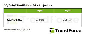
TrendForce's latest investigations have revealed that with consumer demand was concentrated in the first half of the year, leading to the traditional second-half peak season underperforming. The market had expected NAND Flash prices to stabilize in 4Q25. However, HDD shortages and longer lead times have prompted CSPs to quickly redirect storage demand toward QLC enterprise SSDs. This urgent surge in orders has resulted in significant market volatility.

Sandisk was the first to announce a 10% price increase, while Micron paused quotations due to pricing and capacity issues. These events shifted supply-side sentiment from cautious to aggressive. Consequently, NAND Flash contract prices across all categories are expected to generally rise, with an average increase of 5-10% in 4Q25.

Sony Announces the PlayStation Pulse Elevate Wireless Desktop Speakers

We're excited to share a first look at the Pulse Elevate wireless speakers - the newest addition to our lineup of PlayStation audio accessories - which we revealed earlier today during State of Play. Pulse Elevate builds upon the immersive next-level gaming audio experience we introduced to players with Pulse Elite wireless headset and Pulse Explore wireless earbuds, combining powerful technologies like planar magnetic drivers and PlayStation Link into new form factors for players to experience with their favorite games.

As the first wireless speakers developed by Sony Interactive Entertainment, Pulse Elevate fits seamlessly in a PS5, PC, or Mac desktop gaming setup and can be enjoyed on the go with a PlayStation Portal remote player or smartphone. The wireless speakers feature exceptionally lifelike audio, ultra-low latency and lossless PlayStation Link wireless connectivity.

OpenAI and NVIDIA Announce Strategic Partnership to Deploy 10 Gigawatts of NVIDIA Systems

OpenAI and NVIDIA today announced a letter of intent for a landmark strategic partnership to deploy at least 10 gigawatts of NVIDIA systems for OpenAI's next-generation AI infrastructure to train and run its next generation of models on the path to deploying superintelligence. To support this deployment including data center and power capacity, NVIDIA intends to invest up to $100 billion in OpenAI as the new NVIDIA systems are deployed. The first phase is targeted to come online in the second half of 2026 using the NVIDIA Vera Rubin platform.

"NVIDIA and OpenAI have pushed each other for a decade, from the first DGX supercomputer to the breakthrough of ChatGPT," said Jensen Huang, founder and CEO of NVIDIA. "This investment and infrastructure partnership mark the next leap forward—deploying 10 gigawatts to power the next era of intelligence."

TSMC Reportedly Secures 15+ Customers for its "N2" 2 nm Node

TSMC is reportedly handling a significant volume of orders, with 15 or more customers designing on its latest "N2" 2 nm node. According to KLA's Ahmad Khan and Bren Higgins, this N2 node is attracting considerable interest, with 10 of these customers focused on high-performance computing (HPC) designs. Potential clients could include Intel, NVIDIA, AMD, and various startups, while the rest may be developing mobile-optimized designs from companies like Apple, Qualcomm, and MediaTek. "As we're seeing today, the N2 node has about 15 customers working on designs, with around 10 focused on high-performance computing. This is driving rigorous performance requirements," noted KLA's team at a Goldman Sachs conference.

TSMC's N2 node is noted for its high power efficiency and a transistor density of 236.17 million transistors per mm², making it an excellent choice for both HPC/AI and mobile designs. Although TSMC initially planned to implement a backside power delivery network with this node, this feature has been shifted to the A16 node. The N2 will remain a Gate All Around (GAA) FET design to better control transistor gate leakage, moving away from the older FinFET design that has reached its limits with further miniaturization. TSMC has scheduled the commercial launch of the N2 semiconductor node for the second half of 2026, indicating that major technology companies may start adopting this advanced chip technology by early 2027.

STMicroelectronics to Advance Next-Gen Chip Manufacturing Technology with New PLP Pilot Line in France

STMicroelectronics, a global semiconductor leader serving customers across the spectrum of electronics applications, today announced new details regarding the development of the next generations of Panel-Level Packaging (PLP) technology through a pilot line in its Tours site, France, which is expected to be operational in Q3 2026.

PLP is an advanced, automated chip packaging and test process technology bringing increased manufacturing efficiency and reducing costs, and a key enabler for creating the next generation of smaller, more powerful, and cost-effective electronic devices. The large-area carrier in PLP (large rectangular shapes in place of circular wafers) enables higher manufacturing throughput, making it a more efficient solution for high-volume production. Building on its first-generation PLP line in operation in Malaysia and its global technology R&D network, ST plans to develop the next generations of its PLP technology to maintain its technological leadership and extend the use of PLP across many other ST products for automotive, industrial and consumer applications.

HAVIT Opens First Audio Experience Center in Taiwan and Launches New Audio Lineup

HAVIT is proud to announce the grand opening of its first HAVIT Listening Audio Experience Center in Taiwan, bringing immersive sound experiences directly to music lovers.

At the new Audio Experience Center, visitors can enjoy an interactive audio journey. The store is equipped with specialized demo stands, allowing customers to personally test HAVIT's full range of headphones and experience the clarity, depth, and comfort of HAVIT sound before purchase. Whether you're into creation, commuting, or enjoying music every day, the store offers a hands-on way to discover your perfect headphone.

Microsoft Unveils World's Biggest AI Datacenter, Housing Hundreds of Thousands of GPUs

Microsoft announced today that it will bring Fairwater, a purpose-built AI datacenter in Mount Pleasant, Wisconsin, online in early 2026. The new site is designed as the most powerful datacenter on the planet, serving as a hub for next-generation model training and inference. The campus covers 315 acres with roughly 1.2 million square feet across three buildings and will house hundreds of thousands of NVIDIA GB200 and GB300 GPUs linked by fiber, which can reportedly circle the globe 4.5 times. While we don't have information on the exact GPU count, Microsoft claims the installation will deliver about 10x the performance of today's fastest supercomputers for frontier AI workloads. With the fastest already deployed cluster being xAI's Colossus 1, this means that this system could have over half a million "Blackwell" and "Blackwell Ultra" GPUs.

Over 90% of compute capacity will use a closed-loop liquid cooling system that is filled during construction and continuously recirculated, backed by what the company describes as the planet's second-largest water-cooled chiller plant. Around 10% of servers will rely on outside air and switch to water cooling only on the hottest days. Storage and I/O are scaled for exabyte-class datasets, and the buildout involved 46.6 miles of deep foundation piles, 26.5 million pounds of structural steel, 120 miles of medium-voltage underground cable, 72.6 miles of mechanical piping, and an external cooling array that includes 172 20-foot fans.

Samsung Delays V9 QLC NAND Production to H1 2026 Amid Performance Issues

Samsung is running into some unexpected issues with its ninth-generation NAND flash memory technology. The tech giant has been forced to delay full-scale production of its V9 QLC NAND chips until at least the first half of 2026, according to industry reports from ZDNet. Samsung's V9 NAND uses a 280-layer design that first hit mass production back in April 2024. The company started with TLC (triple-level cell) versions that pack 1 TB of storage, then moved on to the more complex QLC (quad-level cell) variants by September last year. But here's where things went sideways. Multiple industry insiders tell ZDNet that those first batches of V9 QLC chips had some fundamental design problems that caused performance issues.

What makes this particularly frustrating for Samsung is that while they still dominate the broader NAND market, they're actually lagging behind when it comes to QLC technology specifically. Their top-tier QLC products are still stuck using older V7 generation technology - they never even bothered releasing a QLC version of their V8 chips. Samsung did show off its next-generation V10-class TLC NAND back in February, boasting over 400 layers and 1 TB capacity. However, they haven't said when we'll actually see these chips in production. Meanwhile, the competition isn't sitting still. Over in Japan, Kioxia has been announcing its own 332-layer V10-class NAND, though they're also still working on getting it ready for mass production. Moreover, SK Hynix recently achieved a breakthrough with its first 321-layer 2 TB QLC NAND chips.

MediaTek's First Chipset Using TSMC's 2nm Process Expected in Late 2026

MediaTek today announced that it is among the first companies to partner with TSMC to successfully develop a chip featuring the enhanced N2P process, taping out MediaTek's flagship system-on-chip (SoC) with volume production expected late next year. Marking a new milestone in the strong partnership between MediaTek and TSMC, this long-standing collaboration continues to yield high performance, power-efficient chipsets for customers in flagship mobile, compute, automotive, data center applications and more.

TSMC's 2 nm technology is the first to adopt nanosheet transistor structure, and N2P represents the next evolution in the 2 nm family, set to deliver improved performance and power efficiency. The first chipset utilizing the new TSMC N2P process is expected to be available in late 2026.

Virtual Boy Returns: Switch Adapter and 14 Classic Titles Headed to Switch in 2026

Thirty years after its debut, Nintendo is reviving its legendary Virtual Boy. During the Nintendo Direct 2025 presentation, the company unveiled an adapter that supports both the Switch and the Switch 2, allowing players to experience the stereoscopic effect on modern screens. Nintendo plans to release two versions: a plastic replica that echoes the original headset and a simplified cardboard edition for budget buyers. Each design lets you slide your console into a built-in cradle so the display aligns with the adapter lenses. The plastic model is priced at $99.99, and the cardboard model at $24.99, with pre-orders opening ahead of the release. The accessories and Virtual Boy collection will arrive on February 17, 2026, and will be sold through Nintendo's online store at launch in the United States and Canada. Playing the collection requires a Nintendo Switch Online subscription with the Expansion Pack tier.

The Nintendo Classics collection will debut with 14 Virtual Boy titles chosen to showcase the system's unusual approach to depth. The launch mix of games includes arcade ports and original experiments, including Virtual Boxing, V-Tetris, Teleroboxer, Mario Clash, Mario's Tennis, and Classic Pinball. Nintendo preserved the original monochrome look while updating the code so the games run on Switch hardware. Beyond nostalgia, this release could jumpstart a wider interest in stereoscopic handheld design. Developers could update mechanics with color, improved depth cues, and modern controls, or craft brand-new stereo-first games. Indie studios might port other niche 3D pieces, and bigger teams could reimagine major franchises in three dimensions. For now, Nintendo offers an affordable way to revisit an odd corner of its past and to test whether players want richer stereoscopic experiences moving forward.

NVIDIA GeForce RTX 50-Series SUPER GPUs Could Arrive at CES 2026

Widespread speculation surrounding the possible launch of the NVIDIA GeForce RTX 50 SUPER series has shifted, with industry sources confirming that the official timeline for the enhanced GPU variants has been moved by a few months. According to Hongxing2020 hardware leaker, known for his ties with GPU AIBs, he claims that the RTX 50 SUPER series has been delayed. Recent online reports have claimed Christmas as the release date; however, these may not be accurate. NVIDIA remains committed to its current RTX 50 Blackwell series for the following months, which continues to operate at full production capacity with no discontinuation plans in sight.

According to VideoCardz, a possible mid-cycle "Blackwell" refresh in the form of SUPER GPUs could hit at CES 2026, when the announcement is expected. NVIDIA plans to increase the memory sizes of key performance-segment and high-end graphics card SKUs to boost their performance in higher resolutions, particularly with ray tracing and neural rendering enabled. Specifically, the company plans to leverage new 24 Gbit density GDDR7 memory chips, which allow it to create memory sizes such as 18 GB over a 192-bit wide memory bus or 24 GB across a 256-bit wide memory bus. Besides the added memory, NVIDIA is expected to increase shader counts and GPU clock speeds marginally.

Intel Confirms "Arrow Lake Refresh" Next Year, "Nova Lake" Scheduled for Late 2026

At the Goldman Sachs Technology conference, Intel confirmed its plan to release an "Arrow Lake Refresh" in 2026, and providing reassurance that the next-generation "Nova Lake" desktop processors will arrive in late 2026. According to John Pitzer, Intel's Corporate Vice President of Corporate Planning & Investor Relations, he reassures that Intel's desktop product portfolio is strong and will remain so as the roadmap materializes. "We've got a couple of holes we've got to fill on the desktop front. But quite frankly, we feel confident in the road map," stated John Pitzer. On Arrow Lake Refresh and Nova Lake, he confirmed that "We'll have a refresh of Arrow Lake next year, which will help start the process on the desktop side, and then we'll conclude that with Nova Lake when we launch late next year into 2027."

The plan for Arrow Lake Refresh isn't currently clear. These desktop CPUs will arrive with the same core count, but supposedly tweaked frequency to extract maximum performance. Initial rumors suggested features like an upgraded NPU, but these were later discarded. For now, all we have to hope for is something similar to the Intel IPO, applied out of the box for Arrow Lake Refresh. This includes fine-tuning the P-core and E-core frequencies, ring-bus speeds, the UPI interconnect, D2D links between tiles, and both PL1 and PL2 power limits. For RAM, IPO raises transfer rates and tightens timings, pushing modules beyond their factory XMP or EXPO profiles, thereby elevating overall performance. If these settings are included out of the box, Intel could justify a refresh without significantly changing the silicon configuration. However, we are yet to see what the company plans as we head into 2026.

China's AI Chip Ambitions Limited by HBM Memory Supply, Notes Report

According to SemiAnalysis, Chinese AI semiconductor buildout faces an unexpected bottleneck that's more critical than manufacturing constraints: high-bandwidth memory shortages. While domestic foundries like SMIC can produce sufficient AI processors, the lack of HBM supply chains has emerged as the primary limitation throttling China's semiconductor ambitions. Huawei's Ascend 910C illustrates this mismatch. The company has foundry capacity to manufacture 805,000 units annually through TSMC, which is a result of stockpiling before the cutoff, as well as SMIC. However, HBM shortages prevent realizing this production potential. Chinese firms accumulated roughly 11.4 million HBM stacks from Samsung before export controls tightened, but these stockpiles won't sustain long-term AI scaling. The memory crunch effectively neutralizes Chinese manufacturing capabilities, giving Western competitors like NVIDIA and AMD a sustained advantage despite Beijing's substantial semiconductor investments.

The path toward HBM independence runs through domestic memory manufacturers like CXMT and the recent collaboration with YMTC. Converting standard DRAM production to HBM manufacturing requires specialized equipment, which is predominantly supplied by Western suppliers, creating another dependency layer. China could achieve competitive HBM3E production by 2026 if current investment trajectories continue and equipment restrictions remain stable. However, this timeline assumes successful technology transfer and uninterrupted access to critical manufacturing tools. If export controls expand to encompass additional HBM-related equipment, the development window could become considerably longer. YMTC is reportedly ready to enter DRAM production and could begin purchasing equipment by late 2025, utilizing its secret weapon, Xtacking technology, one of the most advanced hybrid bonding techniques available. This matters because HBM requires stacking at least 16 memory chips with incredible precision, something YMTC has been doing for years with their NAND products.

Qualcomm CEO: Intel Foundry Not Ready Yet, But Shows Promise

Qualcomm CEO Cristiano Amon, in an interview with Bloomberg Tech, claimed that Intel Foundry isn't yet suitable for its use case, but there is significant potential in the new nodes. According to the CEO, "Intel is not an option today," adding that "We would like Intel to be an option." The CEO discussed how the current Intel Foundry node, likely referring to Intel 18A, is not a suitable option for their mobile chips. However, the primary selling point of the vanilla 18A node isn't mobile, low-power SoCs, but rather mid-range and high-power solutions. "We design all of our chips assuming there's a battery on the other side, not plugged into the wall," said Amon, when asked about the design of their chips and their recent collaboration with German automaker BMW.

Qualcomm will continue to source its low-power SoC from TSMC and Samsung, both of which are skilled in mobile designs. For Intel, most customer attention is drawn to the enhanced 18A nodes, specifically 18A-P, scheduled for rollout in 2026, and 18A-PT, targeted for 2028. This, along with Intel 14A, will be a turning point for the foundry, which seeks to attract customers, including Qualcomm, with these improved nodes. US-based companies are constantly evaluating Intel Foundry services, and over time, these services are becoming increasingly attractive in areas such as packaging, not just advanced manufacturing. Still, the primary goal of Intel Foundry is leading-edge node production, so when/if customers like Qualcomm come, they will need to be ready with satisfying yield and performance figures.

Noctua's Roadmap Update Confirms AIO CLC in Q2 2026

Noctua's upcoming closed-loop all-in-one liquid cooler has finally received a firm release date: the second quarter of 2026. According to the Austrian company roadmap update, which received a September update, we can look forward to more updates soon. Firstly, we can anticipate the arrival of NF-A14x25 G2 chromax.black fans in the Q4 of this year, alongside NH-D15 G2 tower air cooler. Both of these products were originally scheduled for Q3, but Noctua made some final tweaks, and their availability is now expected in Q4. For Q1 in 2026, the company plans to bring the Antec Flux Pro Noctua Edition chassis and the Pulsar Feinman Noctua Edition mouse.

However, the real star of the show is scheduled for Q2 of 2026, when Noctua plans to bring it to the masses. This cooler is based on an Asetek G8 V2 platform that's been heavily optimized by Noctua. Some of the innovations include a pump-noise absorber, SecuFirm 2+ retention module, an 80 mm fan attachment on the pump-block to cool the VRM and memory areas using the Coanda effect, and the inclusion of premium Noctua NF-A14x25 G2 (140 mm) or NF-A12x25 G2 (120 mm) fans, depending on the model. This was also planned for Q1 but has been pushed forward to Q2 as of now. As is the case with Noctua, product delays are a sign that the company is rigorously optimizing the product, so a slight delay will result in better quality, which enthusiasts are accustomed to.

AMD Instinct MI500 UAL256 Mega Pod to Scale up to 256 GPUs, 64 "Verano" CPUs

While AMD hasn't launched its upcoming Instinct MI400 series of accelerators yet, the company has started preparing its supply chain for what comes after. Thanks to SemiAnalysis, we have a clearer picture of what AMD's Instinct MI500 UAL256 rack will look like. At the base of each compute node, there will be a single "Verano" CPU paired with four Instinct MI500 accelerators. With up to 64 nodes, split across two 32-node racks, AMD plans to enable 256 logical GPUs and 64 CPUs per mega pod, working in tandem for advanced AI and HPC workloads. Instinct MI500s UAL256 will be AMD's second-generation rack-scale system, following the upcoming Instinct MI450X IF128 aka "Helios", scheduled for the second half of 2026. The Instinct MI500 UAL256 scale-up mega pod is scheduled to arrive in 2027, just in time for Verano and Instinct MI500 accelerator.

The Instinct MI500 UAL256 scale-up mega pod splits the compute into two 32-rack cabinets, with a single central rack connecting them and hosting 18 switching trays for networking. Each of these networking trays contains four 102.4T "Vulcano" switch ASICs, designed for 800G external throughput, and manufactured on TSMC's 3 nm node. For the central processor, AMD showed few details at its Advancing AI event, which claimed that Verano introduces the "Zen 7" microarchitecture for even higher IPC and support for even newer instruction sets. For now, it's not clear if AMD will increase CPU core counts beyond the up to 256 cores per package of "Venice." Still, we're hearing that Verano will retain the Socket SP7 infrastructure, which means it will likely retain the memory and PCIe interfaces introduced in 2026, such as PCIe Gen 6, UALink, and Ultra Ethernet.

Rapidus 2HP 2 nm Node to Match TSMC N2 on Logic Density

According to Korean analyst Kurnal on X, Rapidus, the Japanese foundry pushing into leading-edge chips, will deliver its upcoming 2 nm process, called 2HP, with a transistor density that rivals the best in the business, even TSMC. The reporting allegedly shows a logic density of 237.31 million transistors per square millimeter for 2HP, essentially matching TSMC's N2, which has 236.17 MTr/mm², and comfortably ahead of Intel's 18A at about 184.21 MTr/mm². Rapidus has focused on high-density standard cells and a single-wafer front-end method that allows engineers to tune runs before scaling. It states that a 2 nm gate-all-around test chip built with ASML EUV tools met its electrical targets. The firm plans to publish process design kits in early 2026 and aims to start high-volume production at its IIM-1 facility in 2027, with monthly output expected to reach roughly 25,000 wafers.

What Rapidus is selling beyond raw density is speed and flexibility. While being a node or two behind TSMC in 2027, the company promises significantly shorter cycle times than traditional batch processes, reducing the typical turnaround from around 120 days to approximately 50 days, and offering extreme "hot lot" pushes down to 15 days for urgent orders. To deliver this, Rapidus is building a custom backend ecosystem with OSATs, EDA vendors, IP providers, and materials partners, and it benefits from government support and interest from major compute players. However, density is only one metric of the new node. Energy efficiency, performance per watt, mature supply chains, and, crucially, repeatable yields will determine whether Rapidus can turn validated test silicon into a reliable, high-volume competitor.

NCSoft Debuts New Shooter Time Takers During Gamescom 2025

Unveiled for the first time during Gamescom's Opening Night Live, MISTIL GAMES' Time Takers is a third-person, team-based survival shooter built around a unique core rule—time as a resource. Players form teams of three, each selecting a "Time Traveler" from a diverse cast of characters drawn from different eras. They must battle other teams in a fight for survival, where only one team can emerge victorious.

In the latest dev video, Yongmin Jo, CEO and Director of Time Takers at MISTIL GAMES, shares the core ideas that make Time Takers unique:
During matches, players collect Time Energy to upgrade skills and equip apps that enhance combat performance. But Time Energy isn't just a power-up—it's also the lifeline that determines individual and team survival. Every second spent or saved becomes a strategic decision.

Dell Technologies Delivers Second Quarter Fiscal 2026 Financial Results

Dell Technologies announces financial results for its fiscal 2026-second quarter. The company also provides guidance for its fiscal 2026 third quarter and full year.

Second-Quarter Summary
  • Record revenue of $29.8 billion, up 19% year over year
  • Operating income of $1.8 billion, up 27% year over year, and non-GAAP operating income of $2.3 billion, up 10%
  • Diluted earnings per share (EPS) of $1.70, up 38% year over year, and record second-quarter non-GAAP diluted EPS of $2.32, up 19%
  • Cash flow from operations of $2.5 billion

AMD Prepares EPYC "Venice" Platform to Break the 1,000 W Power Barrier

The kilowatt era of CPUs is upon us, as AMD is preparing specialized cooling for its next-generation SP7 socket powering EPYC "Venice". During the OCP APAC 2025 Summit in early August, Microloops held a presentation dedicated entirely to system-level cooling using custom high-performance cold plates, cooling distribution units, and much more. However, an interesting tidbit is the mention of AMD and its plan to likely cool CPUs with TDPs ranging from 700 to 1400 W. This marks AMD's first step into a kilowatt-level chip design, requiring kilowatt-level cooling. AMD is preparing to roll out its Zen 6 microarchitecture in 2026, with a server-focused flagship called EPYC "Venice." The new platform is expected to significantly increase core counts, utilizing full-sized Zen 6 cores and an updated I/O subsystem to target much stronger multithreaded throughput. AMD is reportedly configuring Venice to support as many as 256 CPU cores in a single package, a big leap intended to sharpen its position in dense compute environments.

Under the hood, Zen 6 CCDs are planned for TSMC's 2 nm N2 node, while the server I/O die will bring next-generation connectivity with PCIe Gen 6, doubling raw device bandwidth for GPUs, NVMe storage, and high-speed NICs. AMD has also pointed to memory bandwidth claims of up to roughly 1.6 TB/s, which could be achieved through faster DRAM clocks, expanding the memory controller to a 16-channel DDR5 layout from the current 12 channels, or supporting multichannel DIMM formats such as MR-DIMM and MCR-DIMM. Taken together, AMD says Venice will deliver approximately a 70% improvement in multithreaded performance compared to the current EPYC "Turin" family. However, all of that is shaping up to come with a significant power cost, as AMD gears up to cool these chips through customized solutions.

NVIDIA Announces Financial Results for Second Quarter Fiscal 2026

NVIDIA today reported revenue for the second quarter ended July 27, 2025, of $46.7 billion, up 6% from the previous quarter and up 56% from a year ago. NVIDIA's Blackwell Data Center revenue grew 17% sequentially.

There were no H20 sales to China-based customers in the second quarter. NVIDIA benefited from a $180 million release of previously reserved H20 inventory, from approximately $650 million in unrestricted H20 sales to a customer outside of China.

Leaked AMD Roadmap Hints at Zen 6 for Mobile, But Not Until 2027

A pair of leaked partner roadmaps shared by hardware leaker @momomo_us suggests modest change for laptop processors through 2026, followed by a clearer shift in 2027. The documents indicate that AMD will largely be on autopilot next year, with a Zen 5-based refresh called Gorgon Point, which appears to reuse the same core counts, the same 4 nm node, and most of the same NPU and graphics building blocks as Strix Point. That implies only a slight performance improvement, likely due to tighter tuning rather than a new architecture. As a result, high-end mobile parts, such as the Fire Range and the Strix Halo APU, may see little to no refresh in 2026. Zen 6 is coming in 2026 for desktop and server, but for the mobile segment, another year of waiting is on the table.

The leak becomes more interesting for 2027, where two Zen 6 families appear: Gator Range and Medusa Point. Gator Range is positioned as the future elite mobile family and is likely to replace Fire Range; however, the roadmap provides no in-depth technical details beyond the move to Zen 6. Medusa Point is described more concretely. It is said to utilize the FP10 package, be manufactured on a 3 nm process, and ship as a monolithic APU that combines different core types and features stronger iGPU. The listing mentions four full Zen 6 cores, four compact Zen 6c cores, two low-power cores, and roughly eight RDNA / UDNA EUs for on-chip graphics. If true, Medusa Point would target premium laptops with a balance of CPU compute and capable iGPU for gaming and local AI processing. As always with leaked roadmaps, expect changes and wait for official confirmations from AMD.

MSI Teases WoW "Midnight Edition" GeForce RTX 50 SUPER GPU

MSI will release a limited World of Warcraft Midnight edition GeForce RTX graphics card in 2026, the company previewed at Gamescom in Cologne. Blizzard confirmed at the show that the Midnight expansion is due on or before June 30, 2026, and MSI's prototype borrows the expansion's palette with black, white, and blue accents applied to its Gaming Trio design. The collaboration is clearly meant to marry hardware and game lore, with Midnight itself focused on the clash between the Void and the forces of Light, an assault on the Sunwell, and the long-requested addition of player housing.

Given the timing of the WoW update for mid-2026, MSI's special edition is likely destined to arrive alongside NVIDIA's rumored GeForce RTX 50 SUPER refresh also rumored for the next year, which is expected to feature higher core counts, larger memory configurations, and increased power limits for several SKUs. There are already rumors of models with roughly 10,752 CUDA cores and 24 GB of next-generation GDDR7 for an RTX 5080 SUPER, although MSI has not confirmed any technical details for its Midnight card, and the Cologne sample was shown as a concept rather than a final product. Details on pricing, exact specifications, and preorder dates are expected to arrive from the companies closer to the release.

Apple M5 Silicon Adopts LMC Packaging, Paving the Way for CoWoS

According to the well-known Apple insider Ming-Chi Kuo, Apple has reworked a part of its semiconductor supply chain by awarding Taiwan's Eternal Materials exclusive roles in supplying key packaging compounds for its 2026 iPhone and Mac processors. Eternal will supply molding underfill, known as MUF, for the A20 iPhone packages and a liquid molding compound, or LMC, for the high-end M5 Mac processors. TSMC has completed the qualification of these materials and validation for CoWoS use is underway, which could lead to initial shipments in 2026 and a larger role for Eternal in 2027 and 2028. This is noteworthy because it places a Taiwanese materials supplier into a space long dominated by Japanese firms and aligns Apple and TSMC around packaging choices that enable higher memory bandwidth and denser compute layouts.

For the iPhone, transitioning from InFO to wafer-level multi-chip module packaging with MUF reduces material consumption. It simplifies assembly by combining underfill and molding into a single wafer-level process, which is expected to improve yields and lower costs. For Macs, adopting CoWoS-compatible LMC for M5 packages provides better structural integrity, enhanced thermal paths, and more consistent manufacturing outcomes, while leaving full CoWoS adoption for future chip generations. Eternal reportedly beat established Japanese suppliers such as Namics and Nagase to win these orders, which could prompt OSAT partners and other manufacturers to trial the new compounds. It also sets a clear path for Apple to scale more complex multi-die designs in the coming years as it prepares the groundwork for CoWoS and later CoPoS-based processors.

NVIDIA and AMD Customize HBM4 Memory for Next-Generation AI Accelerators

NVIDIA's and AMD's next-generation accelerators will definitely utilize a next-generation HBM4 memory, too. However, interesting news, confirmed by SemiAnalysis, is that these accelerators will utilize a customized HBM memory for the first time. In an HBM stack, consisting of stacked DRAM dies up to a 12-high, connected with TSVs, there is the possibility of embedding an optional base die with customized logic/accelerator circuitry tailored to a specific need. It appears that NVIDIA and AMD are not only exploring this option to gain more performance, but are also actively working on an implementation with a custom base that will push these accelerators ahead of any third-party ASIC solution by a third. Since everyone is trying to grab a bit of market share in the AI ASIC world, NVIDIA and AMD have to innovate their designs to stay ahead constantly.

"We expect NVIDIA and AMD to come out with their custom HBM implementations with HBM4, with other accelerator designers likely to only have a custom base die implementation by HBM4E in the 2027 timeframe," notes the SemiAnalysis post. This means that while ASIC designers, such as Broadcom and MediaTek, will have a working solution in 2027 chips, NVIDIA and AMD will have a working custom HBM4 in 2026 products. For NVIDIA, this is the "Rubin" architecture, supposed to outperform the current "Blackwell" implementation by a wide margin. For AMD, this is the Instinct MI400 series of accelerators, which is coming for the first time in a rack-scale flavor.
Return to Keyword Browsing
Nov 19th, 2026 21:44 CST change timezone

New Forum Posts

Popular Reviews

TPU on YouTube

Controversial News Posts