Monday, September 1st 2025
Rapidus 2HP 2 nm Node to Match TSMC N2 on Logic Density
According to Korean analyst Kurnal on X, Rapidus, the Japanese foundry pushing into leading-edge chips, will deliver its upcoming 2 nm process, called 2HP, with a transistor density that rivals the best in the business, even TSMC. The reporting allegedly shows a logic density of 237.31 million transistors per square millimeter for 2HP, essentially matching TSMC's N2, which has 236.17 MTr/mm², and comfortably ahead of Intel's 18A at about 184.21 MTr/mm². Rapidus has focused on high-density standard cells and a single-wafer front-end method that allows engineers to tune runs before scaling. It states that a 2 nm gate-all-around test chip built with ASML EUV tools met its electrical targets. The firm plans to publish process design kits in early 2026 and aims to start high-volume production at its IIM-1 facility in 2027, with monthly output expected to reach roughly 25,000 wafers.
What Rapidus is selling beyond raw density is speed and flexibility. While being a node or two behind TSMC in 2027, the company promises significantly shorter cycle times than traditional batch processes, reducing the typical turnaround from around 120 days to approximately 50 days, and offering extreme "hot lot" pushes down to 15 days for urgent orders. To deliver this, Rapidus is building a custom backend ecosystem with OSATs, EDA vendors, IP providers, and materials partners, and it benefits from government support and interest from major compute players. However, density is only one metric of the new node. Energy efficiency, performance per watt, mature supply chains, and, crucially, repeatable yields will determine whether Rapidus can turn validated test silicon into a reliable, high-volume competitor.
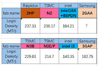
Source:
Kurnal
What Rapidus is selling beyond raw density is speed and flexibility. While being a node or two behind TSMC in 2027, the company promises significantly shorter cycle times than traditional batch processes, reducing the typical turnaround from around 120 days to approximately 50 days, and offering extreme "hot lot" pushes down to 15 days for urgent orders. To deliver this, Rapidus is building a custom backend ecosystem with OSATs, EDA vendors, IP providers, and materials partners, and it benefits from government support and interest from major compute players. However, density is only one metric of the new node. Energy efficiency, performance per watt, mature supply chains, and, crucially, repeatable yields will determine whether Rapidus can turn validated test silicon into a reliable, high-volume competitor.


9 Comments on Rapidus 2HP 2 nm Node to Match TSMC N2 on Logic Density
I was sleepy when i first saw it and though to myself - no wonder Intel and Samsung have trouble with their nodes if they push such aggressive sizes etc.
Later i realized that these were overall density numbers, not individual feature sizes.
Assuming the same cadence of ~two years for a new node it would give them another ~10 years until they reach A1 etc again.
Or they could learn from Google and introduce negative nanometers :laugh:
Naturally the individual gate sizes etc are something like 30nm or something and the overall node name has little to do with reality.
It' s problem of their own making. Same as others in the PC industry starting from a low/high number and then running out (and skipping some) and necessitating a rebrand.
Now I see why we can store 35 bits in an electrondaddy is drunk and needs to learn how to use a measuring stick kinda vibes LOLOLOL
TSMC 3nm family have FinFlex which allows the designer to choose between density/efficiency and performance or both, the numbers for 3nm is for 2-1 fin which is the best case scenario for density.
Cell height for comparison:-
N3E/N3P (2/1) 143 nm.
N2 130 nm.