News Posts matching #5nm

Return to Keyword Browsing

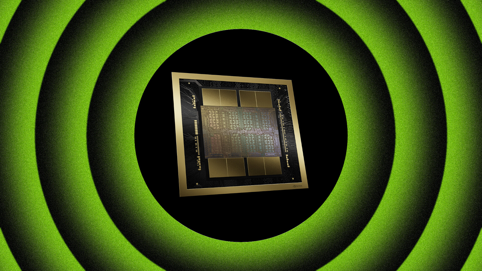
NVIDIA "Blackwell" GeForce RTX to Feature Same 5nm-based TSMC 4N Foundry Node as GB100 AI GPU

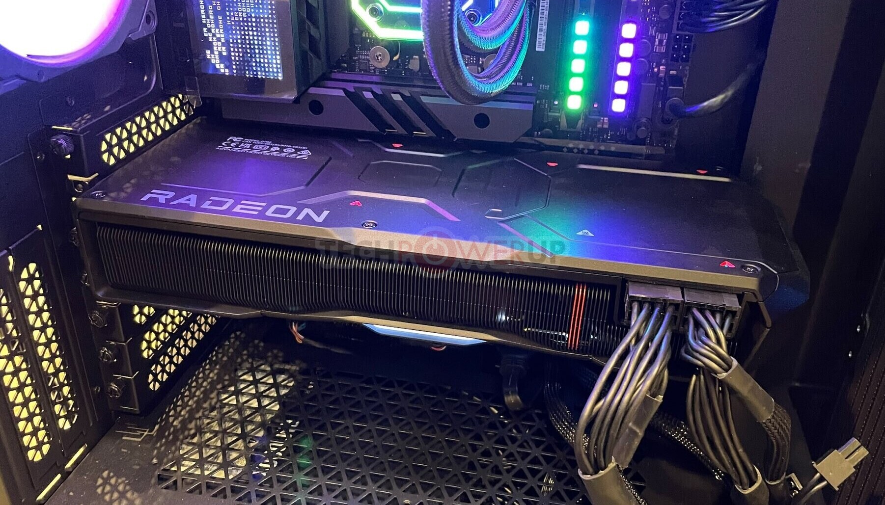
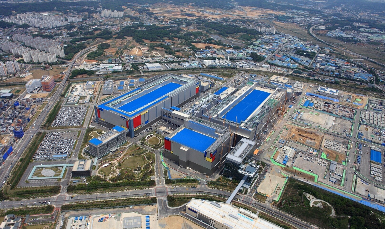
Following Monday's blockbuster announcements of the "Blackwell" architecture and NVIDIA's B100, B200, and GB200 AI GPUs, all eyes are now on its client graphics derivatives, or the GeForce RTX GPUs that implement "Blackwell" as a graphics architecture. Leading the effort will be the new GB202 ASIC, a successor to the AD102 powering the current RTX 4090. This will be NVIDIA's biggest GPU with raster graphics and ray tracing capabilities. The GB202 is rumored to be followed by the GB203 in the premium segment, the GB205 a notch lower, and the GB206 further down the stack. Kopite7kimi, a reliable source with NVIDIA leaks, says that the GB202 silicon will be built on the same TSMC 4N foundry node as the GB100.

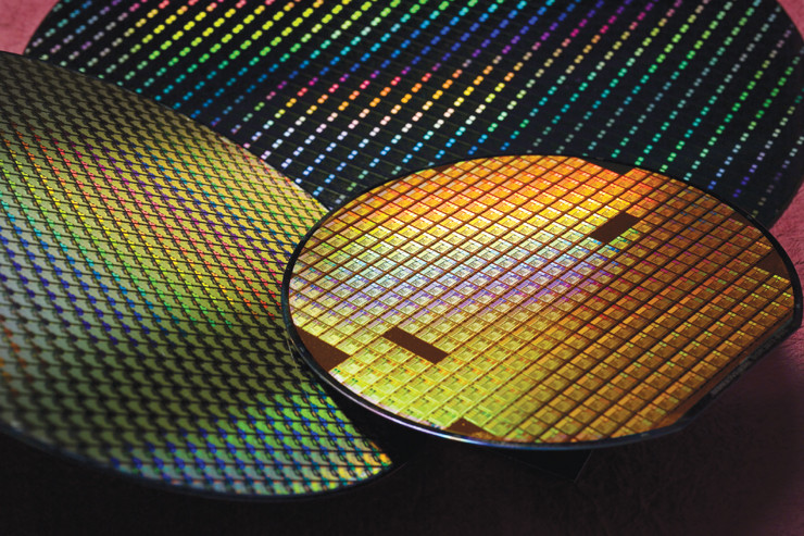
TSMC 4N is a derivative of the company's mainline N4P node, the "N" in 4N stands for NVIDIA. This is a nodelet that TSMC designed with optimization for NVIDIA SoCs. TSMC still considers the 4N as a derivative of the 5 nm EUV node. There is very little public information on the power- and transistor density improvements of the TSMC 4N over TSMC N5. For reference, the N4P, which TSMC regards as a 5 nm derivative, offers a 6% transistor-density improvement, and a 22% power efficiency improvement. In related news, Kopite7kimi says that with "Blackwell," NVIDIA is focusing on enlarging the L1 caches of the streaming multiprocessors (SM), which suggests a design focus on increasing the performance at an SM-level.

Ampere Computing Unveils New AmpereOne Processor Family with 192 Custom Cores

Ampere Computing today announced a new AmpereOne Family of processors with up to 192 single threaded Ampere cores - the highest core count in the industry. This is the first product from Ampere based on the company's new custom core, built from the ground up and leveraging the company's internal IP. CEO Renée James, who founded Ampere Computing to offer a modern alternative to the industry with processors designed specifically for both efficiency and performance in the Cloud, said there was a fundamental shift happening that required a new approach.

"Every few decades of compute there has emerged a driving application or use of performance that sets a new bar of what is required of performance," James said. "The current driving uses are AI and connected everything combined with our continued use and desire for streaming media. We cannot continue to use power as a proxy for performance in the data center. At Ampere, we design our products to maximize performance at a sustainable power, so we can continue to drive the future of the industry."

AMD Makes Radeon Pro W7900 & W7800 Workstation GPUs Official

AMD unveils the most powerful AMD Radeon Pro graphics cards, Offering unique features and leadership performance to tackle heavy to Extreme Professional Workloads - AMD today announced the AMD Radeon PRO W7000 Series graphics, its most-powerful workstation graphics cards to date. The AMD Radeon PRO W7900 and AMD Radeon PRO W7800 graphics cards are built on groundbreaking AMD RDNA 3 architecture, delivering significantly higher performance than the previous generation and exceptional performance-per-dollar compared to the competitive offering. The new graphics cards are designed for professionals to create and work with high-polygon count models seamlessly, deliver incredible image fidelity and color accuracy, and run graphics and compute-based applications concurrently without disruption to workflows.

AMD Radeon PRO W7000 Series graphics cards feature the world's first workstation GPU architecture based on AMD's advanced chiplet design, providing real-world multi-tasking performance and incredible power efficiency. The new graphics cards are also the first professional workstation GPUs to offer the new AMD Radiance Display Engine featuring DisplayPort 2.1 that delivers a superior visual experience, higher resolutions and more available colors than ever before.

EK Ready with AMD Radeon RX 7900 XTX Water Blocks

The long-awaited 3rd of November is here with the latest AMD Radeon RX 7000-series GPUs launch. More good news is that EK, the premium water-cooling gear manufacturer, is ready with EK-Quantum Vector² water blocks for the reference models of the new AMD Radeon RX 7900 XTX GPUs. The new Radeon graphics cards come with a special memory cache dies (MCD) next to the main chip - Graphics Compute Die (GCD). The cooling engine has been modified to cool the MCDs as well, aside from the usual GPU components that are also being cooled, like the VRM, VRAM, Voltage Controllers, and the chip die.

The new Radeon RX 7900 XTX GPUs have GCD that is manufactured in a cutting edge 5 nm process, allowing 54% improvement of performance per watt. While the GPU is efficient, it does still use more power than the previous generation. At 355 W total board power that is packed in a smaller package than ever, with 300 mm² GCD that contains 165% more transistors per mm² than the previous generation. Overall these GPUs feature 58 billion transistors for 61 TFLOPs of performance.

AMD Announces the $999 Radeon RX 7900 XTX and $899 RX 7900 XT, 5nm RDNA3, DisplayPort 2.1, FSR 3.0 FluidMotion

AMD today announced the Radeon RX 7900 XTX and Radeon RX 7900 XT gaming graphics cards debuting its next-generation RDNA3 graphics architecture. The two new cards come at $999 and $899—basically targeting the $1000 high-end premium price point.
Both cards will be available on December 13th, not only the AMD reference design, which is sold through AMD.com, but also custom-design variants from the many board partners on the same day. AIBs are expected to announce their products in the coming weeks.

The RX 7900 XTX is priced at USD $999, and the RX 7900 XT is $899, which is a surprisingly small difference of only $100, for a performance difference that will certainly be larger, probably in the 20% range. Both Radeon RX 7900 XTX and RX 7900 XT are using the PCI-Express 4.0 interface, Gen 5 is not supported with this generation. The RX 7900 XTX has a typical board power of 355 W, or about 95 W less than that of the GeForce RTX 4090. The reference-design RX 7900 XTX uses conventional 8-pin PCIe power connectors, as would custom-design cards, when they come out. AMD's board partners will create units with three 8-pin power connectors, for higher out of the box performance and better OC potential. The decision to not use the 16-pin power connector that NVIDIA uses was made "well over a year ago", mostly because of cost, complexity and the fact that these Radeons don't require that much power anyway.

AMD TSMC's Second Largest Customer for 5nm, More Resilient Than Intel to Face Downturns in the PC Industry: Report

AMD is now TSMC's second largest customer for its 5 nanometer N5 silicon fabrication node, according to a DigiTimes report. The Taiwan-based semiconductor industry observer also reports that AMD is more resilient than Intel in facing any downturns in the PC industry, in the coming few months. PC sales are expected to slump by as much as 15 percent in the near future, but the lower market-share compared to Intel; and the flexibility for AMD to move its CPU chips over to enterprise product to feed the growth in server processor segment, means that the company can ride over a bumpy road in the near future. The lower market-share translates to "lesser pain" from a slump compared to Intel. The report also says that embracing TSMC for processors "just in time" means that AMD has a front-row seat with product performance, time-to-market, yields, and delivery.

AMD is on the anvil of two major product launches on 5 nm, the Ryzen 7000 series "Raphael" desktop processors on August 30 (according to the report), and EPYC "Genoa" server processors in November 2022. The company is planning to refresh its notebook processor lineup in the first half of 2023, with "Dragon Range," and "Phoenix Point" targeting distinct market segments among notebooks. "Dragon Range" is essentially "Raphael" (5 nm chiplet + 6 nm cIOD) on a mobile-optimized BGA package, letting AMD cram up to 16 "Zen 4" cores, and take on Intel's high core-count mobile processors. The iGPU of "Dragon Range" will be basic, since designs based on this chip are expected to use discrete GPUs. "Phoenix Point" is a purpose-built mobile processor with up to 8 "Zen 4" cores, and a powerful iGPU based the RDNA3 architecture.

8-inch Wafer Capacity Remains Tight, Shortages Expected to Ease in 2H23, Says TrendForce

From 2020 to 2025, the compound annual growth rate (CAGR) of 12-inch equivalent wafer capacity at the world's top ten foundries will be approximately 10% with the majority of these companies focusing on 12-inch capacity expansion, which will see a CAGR of approximately 13.2%, according to TrendForce's research. In terms of 8-inch wafers, due to factors such as difficult to obtain equipment and whether capacity expansion is cost-effective, most fabs can only expand production slightly by means of capacity optimization, equating to a CAGR of only 3.3%. In terms of demand, the products primarily derived from 8-inch wafers, PMIC and Power Discrete, are driven by demand for electric vehicles, 5G smartphones, and servers. Stocking momentum has not fallen off, resulting in a serious shortage of 8-inch wafer production capacity that has festered since 2H19. Therefore, in order to mitigate competition for 8-inch capacity, a trend of shifting certain products to 12-inch production has gradually emerged. However, if shortages in overall 8-inch capacity is to be effectively alleviated, it is still necessary to wait for a large number of mainstream products to migrate to 12-inch production. The timeframe for this migration is estimated to be close to 2H23 into 2024.

Samsung Introduces the Industry's First 5nm Processor Powering the Next Generation of Wearables

Samsung Electronics Co., Ltd., a world leader in advanced semiconductor technology, today announced its new wearable processor, the Exynos W920. The new processor integrates an LTE modem and is the first in the industry to be built with an advanced 5-nanometer (nm) extreme ultra-violet (EUV) process node, offering powerful yet efficient performance demanded by next-generation wearable devices.

"Wearables like smartwatches are no longer just a cool gadget to have. They're now a growing part of our lifestyles to keep you fit, safe and alert," said Harry Cho, vice president of System LSI marketing at Samsung Electronics. "With the Exynos W920, future wearables will be able to run applications with visually appealing user interfaces and more responsive user experiences while keeping you connected on the go with fast LTE."

Marvell Extends OCTEON Leadership with Industry's First 5nm DPUs

Marvell today introduced its new OCTEON 10 DPU designed to accelerate and process a broad spectrum of security, networking, and storage workloads required by demanding 5G, cloud, carrier and enterprise datacenter applications. With the increasing shift of workloads to the cloud, complex security requirements and the growing number of edge devices the demand for data centric compute has accelerated. By combining compute with best-in-class hardware accelerators, Marvell's OCTEON 10 DPU offers a significant TCO advantage and features numerous industry firsts. Delivering three times the performance and 50 percent lower power compared to previous generations of OCTEON, the newly announced solution is the first to be designed on a 5 nm process to incorporate Arm Neoverse N2 cores, as well as the first inline artificial intelligence/machine learning (AI/ML) hardware acceleration, the first integrated 1 terabit switch and the first to incorporate vector packet processing (VPP) hardware accelerators.

"To meet and exceed the growing data processing requirements for network, storage, and security workloads, Marvell focused on significant DPU innovations across compute, hardware accelerators, and high speed I/O," said John Sakamoto, vice president of Marvell's Infrastructure Processors Business Unit. "The OCTEON 10 brings compute leadership, supports networking and security workloads exceeding 400G, and incorporates leading edge I/O including DDR5 and PCIe 5.0."

Marvell Launches Industry's First 1.6T Ethernet PHY with 100G PAM4 I/Os in 5nm

Marvell today introduced the industry's first 1.6T Ethernet PHY with 100G PAM4 electrical input/outputs (I/Os) in 5nm. The demand for increased bandwidth in the data center to support massive data growth is driving the transition to 1.6T (Terabits per second) in the Ethernet backbone. 100G serial I/Os play a critical role in the cloud infrastructure to help move data across compute, networking and storage in a power-efficient manner. The new Marvell Alaska C PHY is designed to accelerate the transition to 100G serial interconnects and doubles the bandwidth speeds of the previous generation of PHYs to bring scalability for performance-critical cloud workloads and applications such as artificial intelligence and machine learning.

Marvell's 1.6T Ethernet PHY solution, the 88X93160, enables next-generation 100G serial-based 400G and 800G Ethernet links for high-density switches. The doubling of the signaling rate creates signal integrity challenges, driving the need for retimer devices for high port count switch designs. It's critical that retimer and gearboxes used for these applications are extremely power efficient. Implemented in the latest 5nm node, the Marvell 800GbE PHY provides a 40% savings in I/O power compared to existing 50G PAM4 based I/Os.

Samsung to Build a 5nm EUV Semiconductor Fab in Austin TX

Samsung Electronics plans to build a new cutting-edge semiconductor fab in Austin, Texas, according to an ETimes report. An official announcement to this effect will be made later today, when South Korean President Moon and U.S. President Biden are scheduled to hold their first Summit meeting, in Washington DC. The facility will offer third-party contract manufacturing of semiconductor chips on the 5 nanometer EUV process. Samsung has earmarked an investment of $18 billion toward the construction of this fab, which will be located close to the company's existing foundry in Texas, which manufactures chips on the 14 nm node. Samsung's investment is in response to rising demand of high-volume logic chips by major American firms such as Amazon, Google, Microsoft, and Tesla.

TSMC to Execute Bitmain's Orders for 5nm Crypto-Mining ASICs from Q3-2021

TSMC will be manufacturing next-generation 5 nm ASICs for Bitmain. The company designs purpose-built machines for mining crypto-currency, using ASICs. DigiTimes reports that the 5 nm volume production could kick off form Q3-2021. Bitmain's latest Antminer ASIC-based mining machines announced last month were purported to be up to 32 times faster than a GeForce RTX 3080 at mining Ethereum. Recent history has shown that whenever ASICs catch up or beat GPUs at mining, prices of GPUs tend to drop. With no 5 nm GPUs on the horizon for Q3-2021, one really can expect market pressure from crypto-miners to drop off when Antminers gain traction.

Marvell and TSMC Collaborate to Deliver Industry's Most Advanced Data Infrastructure Portfolio on 5nm Tech

Marvell, a leading provider of data infrastructure semiconductor solutions, today announced an extension of their long term partnership with TSMC (TWSE: 2330; NYSE:TSMC), the world's largest dedicated semiconductor foundry, to deliver a comprehensive silicon portfolio for the data infrastructure market leveraging the industry's most advanced 5 nanometer (nm) process technology. Next-generation infrastructure has never been more critical to the global economy. It's what's keeping the world connected, businesses running and information flowing. With this collaboration, Marvell and TSMC are advancing the essential technology underpinning this infrastructure to provide the storage, bandwidth, speed, and intelligence that tomorrow's digital economy demands - with the added customer benefit of significant energy efficiency. Built in partnership with TSMC on the most advanced process technology currently in volume production, Marvell's new 5 nm portfolio will enable leading-edge silicon innovation for the infrastructure market.

Marvell's breakthrough 5 nm portfolio will provide the essential high-performance compute, networking and security technology required to advance infrastructure development for a multitude of end-market applications. Marvell's Ethernet connectivity solutions enable high-performance, low-power network connectivity, optimized for applications that span cloud data centers to the harsh environment of the automotive market. Marvell's OCTEON platform is the industry's leading Arm-based high-performance compute architecture for embedded infrastructure applications targeting a wide variety of wired and wireless networking equipment including switches, routers, secure gateways, firewalls, and network monitoring solutions. OCTEON is the world's most widely deployed data processing unit (DPU) for data-center scale computing and enables a multitude of acceleration and offload capabilities, including Smart NICs and security accelerators. Featuring optimized and customized 5G processing and baseband capabilities, Marvell's OCTEON Fusion platform is pushing the boundaries of wireless network infrastructure.

TSMC Details 3nm N3, 5nm N5, and 3DFabric Technology

TSMC on Monday kicked off a virtual tech symposium, where it announced its new 12 nm N12e node for IoT edge devices, announced the new 3DFabric Technology, and detailed progress on its upcoming 5 nm N5 and 3 nm N3 silicon fabrication nodes. The company maintains that the N5 (5 nm) node offers the benefits of a full node uplift over its current-gen N7 (7 nm), which recently clocked over 1 billion chips shipped. The N5 node incorporates EUV lithography more extensively than N6/N7+, and in comparison to N7 offers 30% better power at the same performance, 15% more performance at the same power, and an 80% increase in logic density. The company has commenced high-volume manufacturing on this node.

2021 will see the introduction and ramp-up of the N5P node, an enhancement of the 5 nm N5 node, offering a 10% improvement in power at the same performance, or 5% increase in performance at the same power. A nodelet of the N5 family of nodes, called N4, could see risk production in Q4 2021. The N4 node is advertised as "4 nm," although the company didn't get into its iso-power/iso-performance specifics over the N5 node. The next major node for TSMC will be the 3 nm N3 node, with massive 25%-30% improvement in power at the same performance, or 10%-15% improvement in performance at same power, compared to N5. It also offers a 70% logic density gain over N5. 3DFabric technology is a new umbrella term for TSMC's CoWoS (chip on wafer on substrate), CoW (chip on wafer), and WoW (wafer on wafer) 3-D packaging innovations, with which it plans to offer packaging innovations that compete with Intel's various new 3D chip packaging technologies on the anvil.

AMD Confirms "Zen 4" on 5nm, Other Interesting Tidbits from Q2-2020 Earnings Call

AMD late Tuesday released its Q2-2020 financial results, which saw the company rake in revenue of $1.93 billion for the quarter, and clock a 26 percent YoY revenue growth. In both its corporate presentation targeted at the financial analysts, and its post-results conference call, AMD revealed a handful interesting bits looking into the near future. Much of the focus of AMD's presentation was in reassuring investors that [unlike Intel] it is promising a stable and predictable roadmap, that nothing has changed on its roadmap, and that it intends to execute everything on time. "Over the past couple of quarters what we've seen is that they see our performance/capability. You can count on us for a consistent roadmap. Milan point important for us, will ensure it ships later this year. Already started engaging people on Zen4/5nm. We feel customers are very open. We feel well positioned," said president and CEO Dr Lisa Su.

For starters, there was yet another confirmation from the CEO that the company will launch the "Zen 3" CPU microarchitecture across both the consumer and data-center segments before year-end, which means both Ryzen and EPYC "Milan" products based on "Zen 3." Also confirmed was the introduction of the RDNA2 graphics architecture across consumer graphics segments, and the debut of the CDNA scalar compute architecture. The company started shipping semi-custom SoCs to both Microsoft and Sony, so they could manufacture their next-generation Xbox Series X and PlayStation 5 game consoles in volumes for the Holiday shopping season. Semi-custom shipments could contribute big to the company's Q3-2020 earnings. CDNA won't play a big role in 2020 for AMD, but there will be more opportunities for the datacenter GPU lineup in 2021, according to the company. CDNA2 debuts next year.

Samsung Expands its Foundry Capacity with A New Production Line in Pyeongtaek

Samsung Electronics Co., Ltd., a world leader in advanced semiconductor technology, today announced plans to boost its foundry capacity at the company's new production line in Pyeongtaek, Korea, to meet growing global demand for cutting-edge extreme ultraviolet (EUV) solutions.

The new foundry line, which will focus on EUV-based 5 nanometer (nm) and below process technology, has just commenced construction this month and is expected to be in full operation in the second half of 2021. It will play a pivotal role as Samsung aims to expand the use of state-of-the-art process technologies across a myriad of current and next generation applications, including 5G, high-performance computing (HPC) and artificial intelligence (AI).

TSMC Building a 5nm Fab in Arizona as the U.S. Government Gets Involved

It has become a matter of national strategy (or pride) to get TSMC to build a cutting-edge silicon fabrication facility on U.S. soil. Hot on the heals of a report in which TSMC denied it has any plans to build a fab in the U.S., we're learning from a Wall Street Journal that the world's largest independent semiconductor manufacturing company, will build a facility in the U.S. after all. Apparently TSMC will build a silicon fabrication facility in the state of Arizona. The fab will manufacture 5 nm-class chips, to begin with.

TSMC got around to drawing up plans to build a stateside facility after the "involvement" of the State- and Commerce Departments of the U.S. Government. The two are involved not just in coaxing TSMC, but also in the specifics of the planning to get them to the Grand Canyon state. The Donald Trump administration made significant national policy changes with manufacturing, in the wake of the COVID-19 pandemic causing significant wait times in getting silicon products from Asia to the US.

Update 01:25 UTC: TSMC made its U.S. fab plans official with an announcement. Press release and additional commentary below.

TSMC Secures Orders from NVIDIA for 7nm and 5nm Chips

TSMC has reportedly secured orders from NVIDIA for chips based on its 7 nm and 5 nm silicon fabrication nodes, sources tell DigiTimes. If true, it could confirm rumors of NVIDIA splitting its next-generation GPU manufacturing between TSMC and Samsung. The Korean semiconductor giant is commencing 5 nm EUV mass production within Q2-2020, and NVIDIA is expected to be one of its customers. NVIDIA is expected to shed light on its next-gen graphics architecture at the GTC 2020 online event held later this month. With its "Turing" architecture approaching six quarters of market presence, it's likely that the decks are being cleared for a new architecture not just in HPC/AI compute product segment, but also GeForce and Quadro consumer graphics cards. Splitting manufacturing between TSMC and Samsung would help NVIDIA disperse any yield issue arriving from either foundry's EUV node, and give it greater bargaining power with both.

Samsung to Commence 5nm EUV Mass-Production in Q2-2020, Develop 3nm GAAFET Node

Samsung in its Q1-2020 financials release disclosed that the company will commence mass production of chips on its cutting-edge 5 nanometer EUV silicon fabrication process within Q2-2020 (that's before July 2020). This is big, as it lends credence to rumors of NVIDIA secretly developing 5 nm GPUs. Suddenly, it's possible that "Ampere," if not "Hopper," is 5 nm EUV-based, as NVIDIA has chosen Samsung to be its foundry partner for next-generation GPUs.

"In the second quarter, the Company aims to expand EUV leadership, beginning with the start of mass production of 5 nm products, while closely monitoring the uncertain market situation caused by COVID-19," the company states in the release. Samsung also announced that following commencement of mass production on 5 nm, further development of GAAFET (gate all-around FET) 3 nanometer silicon fabrication process will get underway. The company appears to be erring on the side of caution with its forward-looking statements, though. Much of what Samsung does will be dictated by the impact of COVID-19 on the supply chain and market.

Huawei's Loss AMD's Gain, TSMC Develops Special 5nm Node

With Mainland Chinese tech giant Huawei being effectively cut off from contracting Taiwanese TSMC to manufacture its next-generation HiSilicon 5G mobile SoCs, and NVIDIA switching to Samsung for its next-generation GPUs, TSMC is looking to hold on to large high-volume customers besides Apple and Qualcomm, so as to not let them dictate pricing. AMD is at the receiving end of the newfound affection, with the semiconductor firm reportedly developing a new refinement of its 5 nm node specially for AMD, possibly to make Sunnyvale lock in on TSMC for its future chip architectures. A ChainNews report decoded by @chiakokhua sheds light on this development.

AMD is developing its "Zen 4" CPU microarchitecture for a 5 nm-class silicon fabrication node, although the company doesn't appear to have zeroed in on a node for its RDNA3 graphics architecture and CDNA2 scalar compute architecture. In its recent public reveal of the two, AMD chose not to specify the foundry node for the two, which come out roughly around the same time as "Zen 4." It wouldn't be far fetched to predict that AMD and TSMC were waiting on certainty for the new 5 nm-class node's development. There are no technical details of this new node. AMD's demand for TSMC is expected to be at least 20,000 12-inch wafers per month.

TSMC N5P 5nm Node Offers 84-87% Transistor Density Gain Over Current 7nm Node

A WikiChip analysis of TSMC's next-generation 5 nanometer N5P silicon fabrication node estimates a massive 84-87% increase in transistor densities on offer compared to the company's first commercial 7 nm-class node, the N7 (7 nm DUV). The report estimates an 87% transistor-density increase, even though TSMC's own figure is slightly modest, at 84%. TSMC N5P node is expected to commence production later this year. Its precursor, TSMC N5, began risk production earlier this year, with production on the node commencing in April or May, unless derailed by the COVID-19 pandemic. The N5P node provides transistor densities of an estimated 171.3 million transistors per mm² die area, compared to 91.2 mTr/mm² of N7. Apple is expected to be the node's biggest customer in 2020, with the company building its A14-series SoC on it.

Samsung Announces Breakthrough in Building Blocks of 3nm Circuits, Updates Roadmap

Samsung Electronics Co., Ltd., a world leader in advanced semiconductor technology, today announced its ongoing commitment to foundry innovation and service at the Samsung Foundry Forum 2019 USA, providing the silicon community with wide-ranging updates on technology advances that support the most demanding applications of today and tomorrow.

The event, held today in Santa Clara, California, features top Samsung executives and industry experts reviewing progress on semiconductor technologies and foundry platform solutions that enable developments in artificial intelligence (AI), machine learning, 5G networking, automotive, the Internet of Things (IoT), advanced data centers and many other domains.

Intel Courting Samsung to Manufacture Xe GPUs?

Intel's Xe discrete GPU project head Raja Koduri recently visited a Samsung Electronics silicon fabrication facility in Korea at the backdrop of the company's major 5 nm EUV announcement. This sparks speculation that Koduri could be exploring Samsung's portfolio of sub-10 nm contract-manufacturing offerings to mass-produce Xe discrete GPUs. Intel's own foundry business is reeling with mounting pressure from the company's main breadwinner, the client and enterprise processor businesses, to get its 10 nm node on the road. Koduri's GPU would need to leverage higher transistor densities than what Intel's 10 nm could offer, given that rival AMD is already implementing 7 nm, and NVIDIA is expected to go sub-10 nm with its future generation of GPUs.

Samsung Successfully Completes 5nm EUV Development

Samsung Electronics Co., Ltd., a world leader in advanced semiconductor technology, today announced that its 5-nanometer (nm) FinFET process technology is complete in its development and is now ready for customers' samples. By adding another cutting-edge node to its extreme ultraviolet (EUV)-based process offerings, Samsung is proving once again its leadership in the advanced foundry market.

Compared to 7 nm, Samsung's 5 nm FinFET process technology provides up to a 25 percent increase in logic area efficiency with 20 percent lower power consumption or 10 percent higher performance as a result of process improvement to enable us to have more innovative standard cell architecture. In addition to power performance area (PPA) improvements from 7 nm to 5 nm, customers can fully leverage Samsung's highly sophisticated EUV technology. Like its predecessor, 5 nm uses EUV lithography in metal layer patterning and reduces mask layers while providing better fidelity.

TSMC is Ramping Up 7nm Production, 5nm Next Year

At their technology symposium in Taipei, TSMC CEO CC Wei has made remarks, dismissing speculation that their 7 nanometer yield rate was not as good as expected. Rather the company is ramping up production capacity for 7 nm quickly, up 9% from 10.5 million wafers in 2017, to 12 million wafers in 2018. They plan to tape out more than 50 chip designs in 2018, with the majority of the tape outs for AI, GPU and crypto applications, followed by 5G and application processors.

Most of their orders for the 7 nanometer node come from big players like AMD, Bitmain, NVIDIA and Qualcomm. Apple's A12 processor for upcoming iPhones is also a major driver for TSMC's 7 nanometer growth. These orders will be fulfilled in early 2019, so it'll be a bit longer before we have 7 nm processors for the masses.

Next-gen 5 nanometer production will kick off next year, followed by mass production in late 2019 or early 2020. The company will invest as much as USD 25 billion in their new production facilities for this process node.
Return to Keyword Browsing
Apr 26th, 2024 12:18 EDT change timezone

New Forum Posts

Popular Reviews

Controversial News Posts