Monday, March 23rd 2020

TSMC N5P 5nm Node Offers 84-87% Transistor Density Gain Over Current 7nm Node

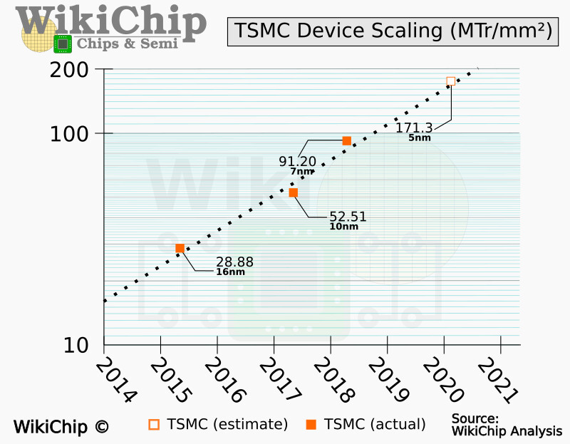
A WikiChip analysis of TSMC's next-generation 5 nanometer N5P silicon fabrication node estimates a massive 84-87% increase in transistor densities on offer compared to the company's first commercial 7 nm-class node, the N7 (7 nm DUV). The report estimates an 87% transistor-density increase, even though TSMC's own figure is slightly modest, at 84%. TSMC N5P node is expected to commence production later this year. Its precursor, TSMC N5, began risk production earlier this year, with production on the node commencing in April or May, unless derailed by the COVID-19 pandemic. The N5P node provides transistor densities of an estimated 171.3 million transistors per mm² die area, compared to 91.2 mTr/mm² of N7. Apple is expected to be the node's biggest customer in 2020, with the company building its A14-series SoC on it.
Source: WikiChip
Add your own comment

11 Comments on TSMC N5P 5nm Node Offers 84-87% Transistor Density Gain Over Current 7nm Node

#1
Fourstaff
Interesting. Intel is falling further behind in fabrication again?
Posted on Reply
#2
btarunr
Editor & Senior Moderator
FourstaffInteresting. Intel is falling further behind in fabrication again?
Appears so. "Zen 4" will be N5P based and "Genoa" processors are slated for either 2H-2021 or 1H-2022.
Posted on Reply
#4
TheGuruStud
Need a meme of intel shitting bricks.
Posted on Reply
#5
ppn
N16 - "28,8 mTr/mm² " - - 25 mTr real
N7 - "91.2 mTr/mm²" - 40-50 mTr real
N5P estimated 171.3 - 60-70 mTr real


So AMD shrinked their GPU by exactly 1,6, where it should have been 3.2x, so what can we expect from 84-85%. less than 42%.
Posted on Reply
#6
Dave65
FourstaffInteresting. Intel is falling further behind in fabrication again?
Seems so. I think Intel should have scrapped 10 nm and maybe even 7 nm and worked on the 5 nm.
Posted on Reply
#7
ARF
ppnN16 - "28,8 mTr/mm² " - - 25 mTr real
N7 - "91.2 mTr/mm²" - 40-50 mTr real
N5P estimated 171.3 - 60-70 mTr real
Those "real" numbers are for the average calculated die transistor density.
While the "estimated" is for all types of memory and cache structures.

Going denser means harder to achieve the clock targets, and by default the designs go less dense in order to keep the clocks higher.

You can have a structure of few transistors ticking at insane clocks.
Posted on Reply
#8
londiste
ppnN16 - "28,8 mTr/mm² " - - 25 mTr real
N7 - "91.2 mTr/mm²" - 40-50 mTr real
N5P estimated 171.3 - 60-70 mTr real
These numbers are a mix of things.

All these production processes have a high density and high performance variations. Manufacturer quoted numbers are obviously high density ones. High performance variation is about 30% less dense. Almost all computer CPUs and GPUs are made on the high performance variation (for obvious reasons), high density tends to be mostly mobile chips.

Edit:
Also, @ARF has a good point that logic is less dense than manufacturer quoted numbers that are usually a variation of memory (SRAM seems to be common). This causes additional reduction in density.
From what both AMD and Intel have said about this, IO seems to be another pain point for scaling as it does not scale as well (probably for obvious reasons).
N5P node is expected to commence production later this year.
N5P is expected to commence risk production in Q2 2020.
Posted on Reply
#9
Kaotik
TSMC's 7nm numbers quoted in the post are for the "(mobile) high density" variant of the process, AMD chips use the "high performance" variant which has way lower density, approximately 2/3rds (estimated numbers for each are ~96.5MTr/mm2 and 66.7MTr/mm^2)
Posted on Reply
#10
ppn
londisteThese numbers are a mix of things.

All these production processes have a high density and high performance variations. Manufacturer quoted numbers are obviously high density ones. High performance variation is about 30% less dense. Almost all computer CPUs and GPUs are made on the high performance variation (for obvious reasons), high density tends to be mostly mobile chips.
Both Samsung and TSMC 7NM performance nodes are estiated around 77 mTt, average transistor in RX 5700 - 40 mTr, only 33 mTr difference. It just doesn't deliver.
16NM performance is 28, average transistor in RX 580 - 25 mTr, only 3 mTr difference.

30% less dense means 65, so the ZEN2 comes really close with 50 mTr because of the L3 cache cells that must be the only 77 mTr element in there.
Posted on Reply
#11
Kaotik
ppnBoth Samsung and TSMC 7NM performance nodes are estiated around 77 mTt, average transistor in RX 5700 - 40 mTr, only 33 mTr difference. It just doesn't deliver.
16NM performance is 28, average transistor in RX 580 - 25 mTr, only 3 mTr difference.

30% less dense means 65, so the ZEN2 comes really close with 50 mTr because of the L3 cache cells that must be the only 77 mTr element in there.
Where did you get the 77 MTr for 7NM performance nodes? TSMCs is 66.7 MTr, not 77 MTr, and Samsung AFAIK reports only one 7nm node, the 7nm EUV which is 95.3 MTr, next node up is 8nm with 61.2 MTr
www.techcenturion.com/7nm-10nm-14nm-fabrication
Posted on Reply
Add your own comment
Apr 26th, 2024 02:50 EDT change timezone

New Forum Posts

Popular Reviews

Controversial News Posts