News Posts matching #7nm

Return to Keyword Browsing

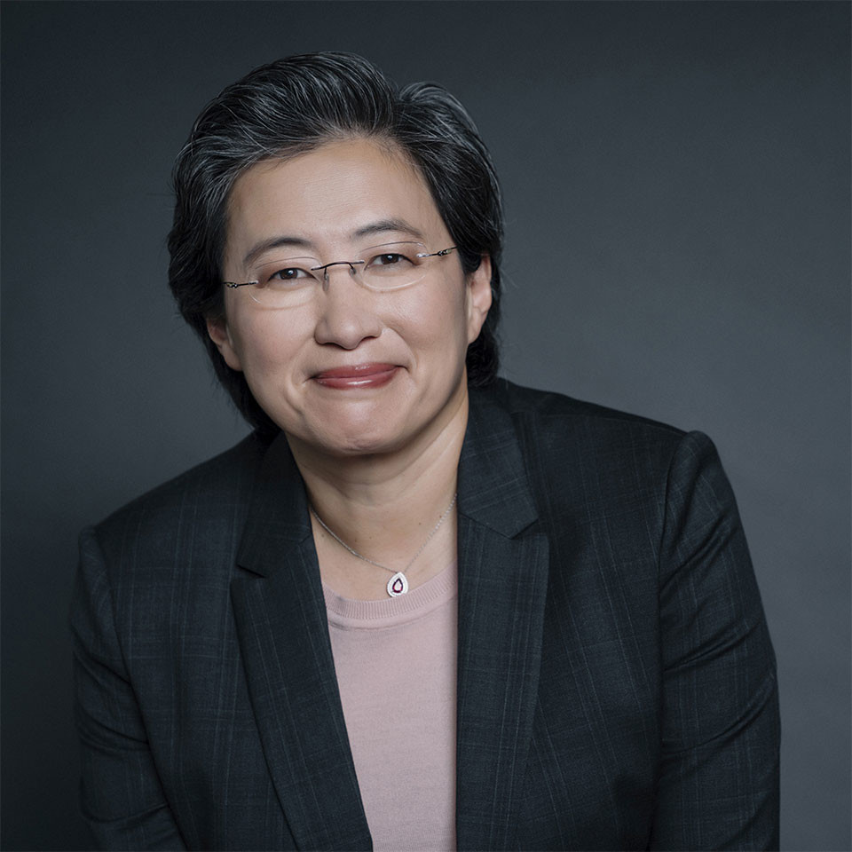
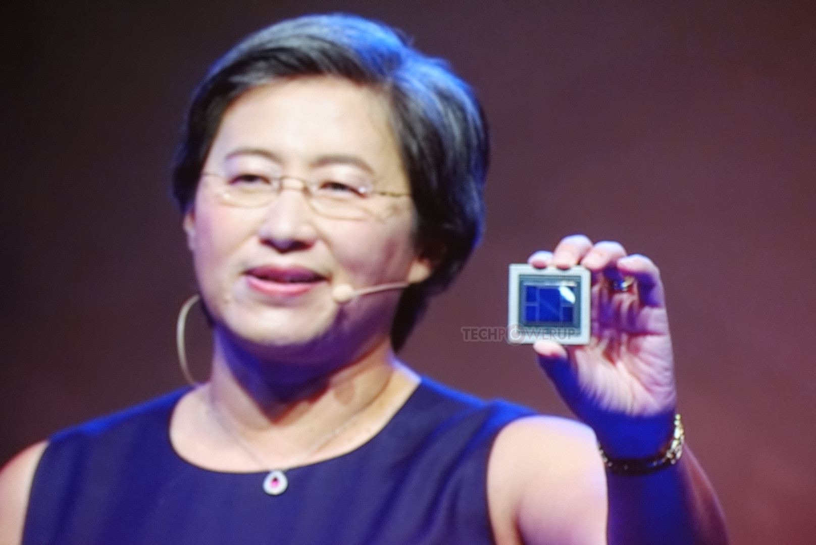
AMD President and CEO Dr. Lisa Su to Deliver COMPUTEX 2019 CEO Keynote

Taiwan External Trade Development Council (TAITRA) announced today that the 2019 COMPUTEX International Press Conference will be held with a Keynote by AMD President and CEO Dr. Lisa Su. The 2019 COMPUTEX International Press Conference & CEO Keynote is scheduled for Monday, May 27 at 10:00 AM in Room 201 of the Taipei International Convention Center (TICC) in Taipei, Taiwan with the keynote topic "The Next Generation of High-Performance Computing".

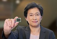
"COMPUTEX, as one of the global leading technology tradeshows, has continued to advance with the times for more than 30 years. This year, for the first time, a keynote speech will be held at the pre-show international press conference," said Mr. Walter Yeh, President & CEO, TAITRA, "Dr. Lisa Su received a special invitation to share insights about the next generation of high-performance computing. We look forward to her participation attracting more companies to participate in COMPUTEX, bringing the latest industry insights, and jointly sharing the infinite possibilities of the technology ecosystem on this global stage."

TSMC 7nm EUV Process to Enter Mass-Production in March 2019

TSMC is giving final touches to set its flagship 7 nanometer EUV (extreme ultraviolet lithography) silicon fabrication node at its highest state of readiness for business, called mass-production. At this state, the node can mass-produce products for TSMC's customers. TSMC had taped out its first 7 nm EUV chips in October 2018. The company will also begin risk-production of the more advanced 5 nm node in April, staying on schedule. Mass production of 5 nm chips could commence in the first half of 2020.

The 7 nm EUV node augments TSMC's 7 nm DUV (deep ultraviolet lithography) node that's been already active since April 2018, and producing chips for AMD, Apple, HiSilicon, and Xilinx. At the turn of the year, 7 nm DUV made up 9 percent of TSMC's shipments. With the new node going online, 7 nm (DUV + EUV) could make up 25 percent of TSMC's output by the end of 2019.

GIGABYTE Announces its Radeon VII Graphics Card

GIGABYTE, the world's leading premium gaming hardware manufacturer, today announced the launch of Radeon VII HBM2 16G, the latest Radeon VII graphics cards built upon the world's first 7nm gaming GPU. Based on the enhanced second-generation AMD 'Vega' architecture, Radeon VII is equipped with 3840 stream processors and 16GB of ultra-fast HBM2 memory (second-generation High-Bandwidth Memory). It is designed to deliver exceptional performance and amazing experiences for the latest AAA, e-sports and Virtual Reality (VR) titles, demanding 3D rendering and video editing applications, and next-generation compute workloads.

According to the AMD official website, the Radeon VII graphics card enables high-performance gaming and ultra-high quality visuals. Ground-breaking 1 TB/s memory bandwidth and a 4,096-bit memory interface paves the way for ultra-high resolution textures, hyper-realistic settings and life-like characters. With the high speeds of today's graphics cards, framerates often exceed the monitor refresh rate, causing stuttering and tearing.

MSI Announces AMD Radeon VII Graphics Card

MSI is proud to officially announce AMD Radeon VII, the world's first 7nm gaming graphics card. The all-new Radeon VII is designed to provide exceptional performance and amazing experiences for the latest AAA, esports and VR titles, demanding 3D rendering and video editing applications, and next-generation compute workloads.

"AMD Radeon VII is the highest-performance gaming graphics card we have ever created," said Scott Herkelman, corporate vice president and general manager, Radeon Technologies Group at AMD. "It is designed for gamers, creators and enthusiasts who demand ultra-high quality visuals, uncompromising performance and immersive gaming experiences."

AMD Updates Wafer Supply Agreement with GlobalFoundries to Free Itself of "7nm Tax"

AMD in its Q4-2018 Earnings Report disclosed that it has amended its Wafer Supply Agreement (WSA) with GlobalFoundries that frees it from paying a "7 nanometer tax." Under the older version of WSA, AMD would have had to pay a penalty to GlobalFoundries if it sourced processors from any other semiconductor foundry. The company got preferential pricing in return for the exclusivity. With GlobalFoundries discontinuing development of cutting-edge processes such as 7 nm and 5 nm, it makes sense for AMD to seek out other foundry partners, such as TSMC, and an amendment to the WSA was needed. With this amendment in place, AMD can go ahead and source 7 nm dies from TSMC without paying penalties to GlobalFoundries (GloFo).

With its "Zen 2" microarchitecture, AMD is going big on multi-chip modules, in which only those components that can tangibly benefit from the switch to the 7 nm node, namely the CPU cores, would be built on 7 nm dies, called "CPU chiplets," while components that don't need the miniaturization just yet, such as the processor's memory controller, PCIe root-complex, etc., will be built on separate dies called "I/O controllers." These dies will continue to be 14 nm, and likely supplied by GloFo. Final packaging of 7 nm CPU chiplets from TSMC, and 14 nm I/O controllers from GloFo, will happen at GloFo's facilities in China or Malaysia. AMD in its amendment committed to purchasing 14 nm and 12 nm chips from GloFo between 2019 and 2021, which means the MCM approach to processors is here to stay.

NVIDIA CEO Jensen Huang on Radeon VII: "Underwhelming (...) the Performance is Lousy"; "Freesync Doesn't Work"

PC World managed to get a hold of NVIDIA CEO Jensen Huang, picking his thoughts on AMD's recently announced Radeon VII. Skirting through the usual amicable, politically correct answers, Jensen made his thoughts clear on what the competition is offering to compete with NVIDIA's RTX 2000 series. The answer? Vega VII is an "underwhelming product", because "The performance is lousy and there's nothing new. [There's] no ray tracing, no AI. It's 7nm with HBM memory that barely keeps up with a 2080. And if we turn on DLSS we'll crush it. And if we turn on ray tracing we'll crush it." Not content on dissing the competition's product, Jensen Huang also quipped regarding AMD's presentation and product strategy, saying that "It's a weird launch, maybe they thought of it this morning."

IBM Expands Strategic Partnership with Samsung to Include 7nm Chip Manufacturing

IBM today announced an agreement with Samsung to manufacture 7-nanometer (nm) microprocessors for IBM Power Systems , IBM Z and LinuxONE , high-performance computing (HPC) systems, and cloud offerings. The agreement combines Samsung's industry-leading semiconductor manufacturing with IBM's high-performance CPU designs. This combination is being designed to drive unmatched systems performance, including acceleration, memory and I/O bandwidth, encryption and compression speed, as well as system scaling. It positions IBM and Samsung as strategic partners leading the new era of high-performance computing specifically designed for AI.

"At IBM, our first priority is our clients," said John Acocella, Vice President of Enterprise Systems and Technology Development for IBM Systems. "IBM selected Samsung to build our next generation of microprocessors because they share our level of commitment to the performance, reliability, security, and innovation that will position our clients for continued success on the next generation of IBM hardware."

Intel 7nm EUV Node Back On Track, 2x Transistor Densities Over 10nm

There could be light at the end of the tunnel for Intel's silicon fabrication business after all, as the company reported that its 7 nanometer silicon fabrication node, which incorporates EUV (extreme ultraviolet) lithography, is on track. The company stressed in its Nasdaq Investors' Conference presentation that its 7 nm EUV process is de-linked from its 10 nm DUV (deep ultraviolet) node, and that there are separate teams working on their development. The 10 nm DUV node is qualitatively online, and is manufacturing small batches of low-power mobile "Cannon Lake" Core processors.

Cannon Lake is an optical shrink of the "Skylake" architecture to the 10 nm node. Currently there's only one SKU based on it, the Core i3-8121U. Intel utilized the electrical gains from the optical shrink to redesign the client-segment architecture's FPU to support the AVX-512 instruction-set (although not as feature-rich as the company's enterprise-segment "Skylake" derivatives). The jump from 10 nm DUV to 7 nm EUV will present a leap in transistor densities, with Intel expecting nothing short of a doubling. 10 nm DUV uses a combination of 193 nm wavelength ultraviolet lasers and multi-patterning to achieve its transistor density gains over 14 nm++. The 7 nm EUV node uses an extremely advanced 135 nm indirect laser, reducing the need for multi-patterning. The same laser coupled with multi-patterning could be Intel's ticket to 5 nm.

AMD President and CEO Dr. Lisa Su Bestowed with GSA Exemplary Leadership Award

Global Semiconductor Alliance (GSA) will honor industry visionary and innovator Dr. Lisa Su, President and CEO, Advanced Micro Devices (AMD), with the prestigious Dr. Morris Chang Exemplary Leadership Award at its highly-anticipated Annual Awards Dinner to be held in Santa Clara, California, on December 6, 2018.

Established in 1999, the Dr. Morris Chang Exemplary Leadership Award recognizes individuals for their exceptional contributions, exemplifying how their vision and global leadership have transformed and elevated the entire semiconductor industry. The selection of Dr. Su is based on her ongoing technological contributions, exceptional business acumen, status as a positive and inspiring role model, and wide ranging respect among the technology industry and business community.

AMD Unveils World's First 7 nm GPUs - Radeon Instinct MI60, Instinct MI50

AMD today announced the AMD Radeon Instinct MI60 and MI50 accelerators, the world's first 7nm datacenter GPUs, designed to deliver the compute performance required for next-generation deep learning, HPC, cloud computing and rendering applications. Researchers, scientists and developers will use AMD Radeon Instinct accelerators to solve tough and interesting challenges, including large-scale simulations, climate change, computational biology, disease prevention and more.

"Legacy GPU architectures limit IT managers from effectively addressing the constantly evolving demands of processing and analyzing huge datasets for modern cloud datacenter workloads," said David Wang, senior vice president of engineering, Radeon Technologies Group at AMD. "Combining world-class performance and a flexible architecture with a robust software platform and the industry's leading-edge ROCm open software ecosystem, the new AMD Radeon Instinct accelerators provide the critical components needed to solve the most difficult cloud computing challenges today and into the future."

GLOBALFOUNDRIES Introduces Avera Semi

GLOBALFOUNDRIES today announced the establishment of Avera Semiconductor LLC, a wholly owned subsidiary dedicated to providing custom silicon solutions for a broad range of applications. Avera Semi will leverage deep ties with GF to deliver ASIC offerings on 14/12nm and more mature technologies while providing clients new capabilities and access to alternate foundry processes at 7nm and beyond.

Avera Semi is built upon an unrivaled legacy of ASIC expertise, tapping into a world-class team that has executed more than 2,000 complex designs in its 25-year history. With more than 850 employees, annual revenues in excess of $500 million, and over $3 billion in 14nm designs in execution, Avera Semi is well positioned to serve clients developing products across a wide range of markets, including wired and wireless networking, data centers and storage, artificial intelligence and machine learning, and aerospace and defense.

AMD Zen 2 GNU Compiler Patch Published, Exposes New Instruction Sets

With a November deadline for feature freeze fast approaching, GNU toolchain developers are now adding the last feature additions to GCC 9.0 (GNU Compiler Collection). Ahead of that deadline, AMD has released their first basic patch adding the "znver2" target and therefore Zen 2 support to GCC. While the patch uses the same cost tables and scheduler data as Znver1, it does feature three new instructions that will be available to AMD's next-gen CPUs which include; Cache Line Write Back (CLWB), Read Processor ID (RDPID), and Write Back and Do Not Invalidate Cache (WBNOINVD).

These three instructions are the only ones that have been found thus far by digging through the current code. Taking into account this is the first patch it can be considered a jumping off point, making sure that the GCC 9.1 stable update, which comes out in 2019, has support for Zen 2. Further optimizations and instructions may be implemented in the future. This is likely since AMD has yet to update the scheduler cost tables and by extension means they may not want to reveal everything about Zen 2 just yet. You could say AMD is for now playing it safe, at least until their 7nm EPYC 2 processors launch in 2019.

AMD Vega 20 Possible Performance Spotted in Final Fantasy XV Benchmark

It would appear AMD's 7nm Vega 20 has been benchmarked in Final Fantasy XV. While the details are scarce, what we do know is the hardware device ID 66AF:C1 can be linked to Vega 20 via the Linux patches back in April. Now considering AMD has not confirmed any 7nm Vega graphics cards for consumers, It is more likely this version is an engineering sample for the new Radeon Instinct or Pro series cards.

Samsung Electronics Starts Production of EUV-based 7nm LPP Process

Samsung Electronics, a world leader in advanced semiconductor technology, today announced that it has completed all process technology development and has started wafer production of its revolutionary process node, 7LPP, the 7-nanometer (nm) LPP (Low Power Plus) with extreme ultraviolet (EUV) lithography technology. The introduction of 7LPP is a clear demonstration of Samsung Foundry's technology roadmap evolution and provides customers with a definite path to 3nm. The commercialization of its newest process node, 7LPP gives customers the ability to build a full range of exciting new products that will push the boundaries of applications such as 5G, Artificial Intelligence, Enterprise and Hyperscale Datacenter, IoT, Automotive, and Networking.

"With the introduction of its EUV process node, Samsung has led a quiet revolution in the semiconductor industry," said Charlie Bae, executive vice president of foundry sales and marketing team at Samsung Electronics. "This fundamental shift in how wafers are manufactured gives our customers the opportunity to significantly improve their products' time to market with superior throughput, reduced layers, and better yields. We're confident that 7LPP will be an optimal choice not only for mobile and HPC, but also for a wide range of cutting-edge applications."

AMD Fast-tracks 7nm "Navi" GPU to Late-2018 Alongside "Zen 2" CPU

AMD is unique in the world of computing as the only company with both high-performance CPU and GPU products. For the past several years we have been executing our multi-generational leadership product and architectural roadmap. Just in the last 18 months, we successfully introduced and ramped our strongest set of products in more than a decade and our business has grown dramatically as we gained market share across the PC, gaming and datacenter markets.

The industry is at a significant inflection point as the pace of Moore's Law slows while the demand for computing and graphics performance continues to grow. This trend is fueling significant shifts throughout the industry and creating new opportunities for companies that can successfully bring together architectural, packaging, system and software innovations with leading-edge process technologies. That is why at AMD we have invested heavily in our architecture and product roadmaps, while also making the strategic decision to bet big on the 7nm process node. While it is still too early to provide more details on the architectural and product advances we have in store with our next wave of products, it is the right time to provide more detail on the flexible foundry sourcing strategy we put in place several years ago.

AMD Chip Manufacturing to Lay Solely With TSMC On, After 7 nm - And Why It's not a Decision, but a Necessity

It's been a tumultuous few days for AMD, as the company has seen Jim Anderson, Computing and Graphics Group leader after the departure of Raja Koduri, leave the company, at a time of soaring share value for the company (hitting $25.26 and leaving short positions well, short, by $2.67 billion.) However, there's one particular piece of news that is most relevant for the company: Globalfoundries' announcement to stop all ongoing development on the 7 nm node.

This is particularly important for a variety of reasons. The most important one is this: Globalfoundries' inability to execute on the 7 nm node leaves AMD fully free to procure chips and technology from competing foundries. If you remember, AMD's spin-off of GlobalFoundries left the former with the short end of the stick, having to cater to GlobalFoundries' special pricing, and paying for the privilege of accessing other foundries' inventories. Of course, the Wafer Supply Agreement (WSA) that is in place will have to be amended - again - but the fact is this: AMD wants 7 nm products, and GlobalFoundries can't provide.
To the forumites: this piece is marked as an editorial

GlobalFoundries Puts its 7 nm Program on Hold Indefinitely

GLOBALFOUNDRIES today announced an important step in its transformation, continuing the trajectory launched with the appointment of Tom Caulfield as CEO earlier this year. In line with the strategic direction Caulfield has articulated, GF is reshaping its technology portfolio to intensify its focus on delivering truly differentiated offerings for clients in high-growth markets.

GF is realigning its leading-edge FinFET roadmap to serve the next wave of clients that will adopt the technology in the coming years. The company will shift development resources to make its 14/12nm FinFET platform more relevant to these clients, delivering a range of innovative IP and features including RF, embedded memory, low power and more. To support this transition, GF is putting its 7nm FinFET program on hold indefinitely and restructuring its research and development teams to support its enhanced portfolio initiatives. This will require a workforce reduction, however a significant number of top technologists will be redeployed on 14/12nm FinFET derivatives and other differentiated offerings.

Intel Stuck with 14nm Processors Till Holiday 2019

Wrap your head around this: at some point in 2019, AMD will be selling 7 nm processors while Intel sells 14 nm processors. That how grim Intel's 10 nanometer silicon fabrication process development is looking. In the Q&A session of its Q2-2018 Earnings Call, Intel stated that the first products based on its 10 nm process will arrive only by Holiday 2019, making 14 nm micro-architectures hold the fort for not just the rest of 2018, but also most of 2019. In the client-segment, Intel is on the verge of launching its 9th generation Core "Whiskey Lake" processor family, its 5th micro-architecture on the 14 nm node after "Broadwell," "Skylake," "Kaby Lake," and "Coffee Lake."

It's likely that "Whiskey Lake" will take Intel into 2019 after the company establishes performance leadership over 12 nm AMD "Pinnacle Ridge" with a new round of core-count increases. Intel is also squeezing out competitiveness in its HEDT segment by launching new 20-core and 22-core LGA2066 processors; and a new platform with up to 28 cores and broader memory interface. AMD, meanwhile, hopes to have the first 7 nm EPYC processors out by late-2018. Client-segment products based on its architecture, however, will follow the roll-out of these enterprise parts. We could see a point in 2019 when AMD launches its 7 nm 3rd generation Ryzen processors in the absence of competing 10 nm Core processors from Intel. Posted below is an Intel slide from 2013, when the company was expecting 10 nm rollout by 2015. That's how much its plans have derailed.

No 16-core AMD Ryzen AM4 Until After 7nm EPYC Launch (2019)

AMD in its Q2-2018 investors conference call dropped more hints at when it plans to launch its 3rd generation Ryzen processors, based on its "Zen2" architecture. CEO Lisa Su stated in the Q&A session that rollout of 7 nm Ryzen processors will only follow that of 7 nm EPYC (unlike 1st generation Ryzen preceding 1st generation EPYC). What this effectively means is that the fabled 16-core die with 8 cores per CCX won't make it to the desktop platform any time soon (at least not in the next three quarters, certainly not within 2018).

AMD CEO touched upon the development of the company's 7 nm "Rome" silicon, which will be at the heart of the company's 2nd generation EPYC processor family. 2nd generation EPYC, as you'd recall from our older article, is based on 7 nm "Zen2" architecture, and not 12 nm "Zen+." 3rd generation Ryzen is expected to be based on "Zen2." As of now, the company is said to have completed tape-out of "Rome," and is sending samples out to its industry partners for further testing and validation. The first EPYC products based on this will begin rolling out in 2019. The 7 nm process is also being used for a new "Vega" based GPU, which has taped out, and will see its first enterprise-segment product launch within 2018.

Samsung Foundry and Arm Expand Collaboration to Drive High-Performance Computing Solutions

Samsung Electronics, a world leader in advanced semiconductor technology, today announced that its strategic foundry collaboration with Arm will be expanded to 7/5-nanometer (nm) FinFET process technology to remain a step ahead in the era of high-performance computing. Based on Samsung Foundry's 7LPP (7nm Low Power Plus) and 5LPE (5nm Low Power Early) process technologies, the Arm Artisan physical IP platform will enable 3GHz+ computing performance for Arm's Cortex -A76 processor.

Samsung's 7LPP process technology will be ready for its initial production in the second half of 2018. The first extreme ultra violet (EUV) lithography process technology, and its key IPs, are in development and expected to be completed by the first half of 2019. Samsung's 5LPE technology will allow greater area scaling and ultra-low power benefits due to the latest innovations in 7LPP process technology.

TSMC is Ramping Up 7nm Production, 5nm Next Year

At their technology symposium in Taipei, TSMC CEO CC Wei has made remarks, dismissing speculation that their 7 nanometer yield rate was not as good as expected. Rather the company is ramping up production capacity for 7 nm quickly, up 9% from 10.5 million wafers in 2017, to 12 million wafers in 2018. They plan to tape out more than 50 chip designs in 2018, with the majority of the tape outs for AI, GPU and crypto applications, followed by 5G and application processors.

Most of their orders for the 7 nanometer node come from big players like AMD, Bitmain, NVIDIA and Qualcomm. Apple's A12 processor for upcoming iPhones is also a major driver for TSMC's 7 nanometer growth. These orders will be fulfilled in early 2019, so it'll be a bit longer before we have 7 nm processors for the masses.

Next-gen 5 nanometer production will kick off next year, followed by mass production in late 2019 or early 2020. The company will invest as much as USD 25 billion in their new production facilities for this process node.

AMD to Polevault Zen+, Head Straight to 7nm Zen2 for EPYC

AMD in its Computex 2018 address earlier today, mention that its second-generation EPYC enterprise processors will be based on its 7 nanometer "Zen 2" architecture, and not 12 nm "Zen+." The company has the 7 nm silicon ready in its labs, and will begin sampling within the second half of 2018. The first products could launch in 2019, after validations. Besides improved energy-efficiency, the 12 nm "Zen+" architecture features a minor 3-5 percent IPC uplift thanks to improved multi-core clock-speed boosting, and faster caches. "Zen 2," on the other hand, presents AMD with the opportunity to make major design changes to its silicon to achieve higher IPC uplifts. The 7 nm process introduces significant transistor density uplifts over the current process. AMD is in the process of building 4-die multi-chip modules using the 12 nm "Pinnacle Ridge" silicon for its 2nd generation Ryzen Threadripper HEDT client processor family.

AMD Demonstrates 7nm Radeon Vega Instinct HPC Accelerator

AMD demonstrated the world's first GPU built on the 7 nanometer silicon fabrication process, a Radeon Vega Instinct HPC/AI accelerator, with a 7 nm GPU based on the "Vega" architecture, at its heart. This chip is an MCM of a 7 nm GPU die, and 32 GB HBM2 memory stacks over four stacks (4096-bit memory bus width). It's also the first product to feature a removable InfinityFabric interface (competition to NVIDIA's NVLink interface). There will also be variants based on the common PCI-Express 3.0 x16. The card supports hardware virtualization and new deep-learning ops.

AMD to Begin Sampling 7nm "Zen 2" Processors Within 2018 for a 2019 Launch

It looks like AMD's processor product launch cycle is on steroids, and keeping up (or even ahead) of Intel. After launching the first 12 nm processor architecture with "Zen+," the company is giving final touches to what it hopes to be the world's first 7 nanometer processor architecture, with "Zen 2." The company will reportedly begin sampling the chip within 2018, to enable volume production and market launch in 2019. Speaking at an investors conference call following the company's Q1-2018 Results release, AMD CEO Dr. Lisa Su confirmed the 7 nm roll-out strategy of her company.

"We have a 7nm GPU based on Vega that we'll sample later this year. We have a 7nm server CPU that we'll sample later this year. And then, obviously, we have a number of products that are planned for 2019 as well. So it's a very, very busy product season for us. But we're pleased with the sort of the execution on the product roadmap," Dr. Su said. Unlike Zen+, Zen 2 is a major update to the company's processor micro-architecture, and presents the company with opportunities to improve several silicon-level specifications, such as the number of cores per CCX, the IPC of each core, the core-count of the die, the cache hierarchy, and the overall energy-efficiency.

Qualcomm to Build Snapdragon 5G SoCs on Samsung 7nm LPP EUV Process

Samsung Electronics, a world leader in advanced semiconductor technology, and Qualcomm Technologies, Inc., a subsidiary of Qualcomm Incorporated, today announced the intention to expand their decade-long foundry relationship into EUV (extreme ultra violet) lithography process technology, including the manufacture of future Qualcomm Snapdragon 5G mobile chipsets using Samsung's 7-nanometer (nm) LPP (Low Power Plus) EUV process technology.

Using 7LPP EUV process technology, Snapdragon 5G mobile chipsets will offer a smaller chip footprint, giving OEMs more usable space inside upcoming products to support larger batteries or slimmer designs. Process improvements, combined with a more advanced chip design, are expected to bring significant improvements in battery life.
Return to Keyword Browsing
Apr 26th, 2024 20:44 EDT change timezone

New Forum Posts

Popular Reviews

Controversial News Posts