News Posts matching #CoWoS

Return to Keyword Browsing

NVIDIA May Cut TSMC Chip Orders Amid Mounting Pressure, Report Claims

NVIDIA may be slowing down its chip orders at TSMC, according to a new report from Taiwan's Commercial Times. The outlet cites unnamed supply chain sources but doesn't name a product, node, size, or timeline. Neither NVIDIA nor TSMC have commented so far, and the claims are single-sourced for now. The report frames this as NVIDIA being squeezed from inside and out. On the inside, there's Jensen Huang's November 8 email to staff, in which he apologized for an extramarital affair, and the board's independent investigation into reports that he was targeted by a foreign intelligence effort. The board has said it has no reason to believe national security or NVIDIA secrets were compromised.

The outside pressure mostly comes down to export controls. The report points to tighter export reviews and H200 chips reportedly stockpiled in Hong Kong, both of which it says raise the risk of NVIDIA scaling back orders. It also cites foreign media reports suggesting that some firms approved to handle H200 could be shell companies, which feeds concerns that chips might reach China through fronts like these or middlemen in other countries. The report presents that as a suspicion rather than a finding, and if cuts do happen, upstream suppliers such as TSMC and ASE are the most exposed.

TSMC is Reportedly Considering 3D DRAM Production

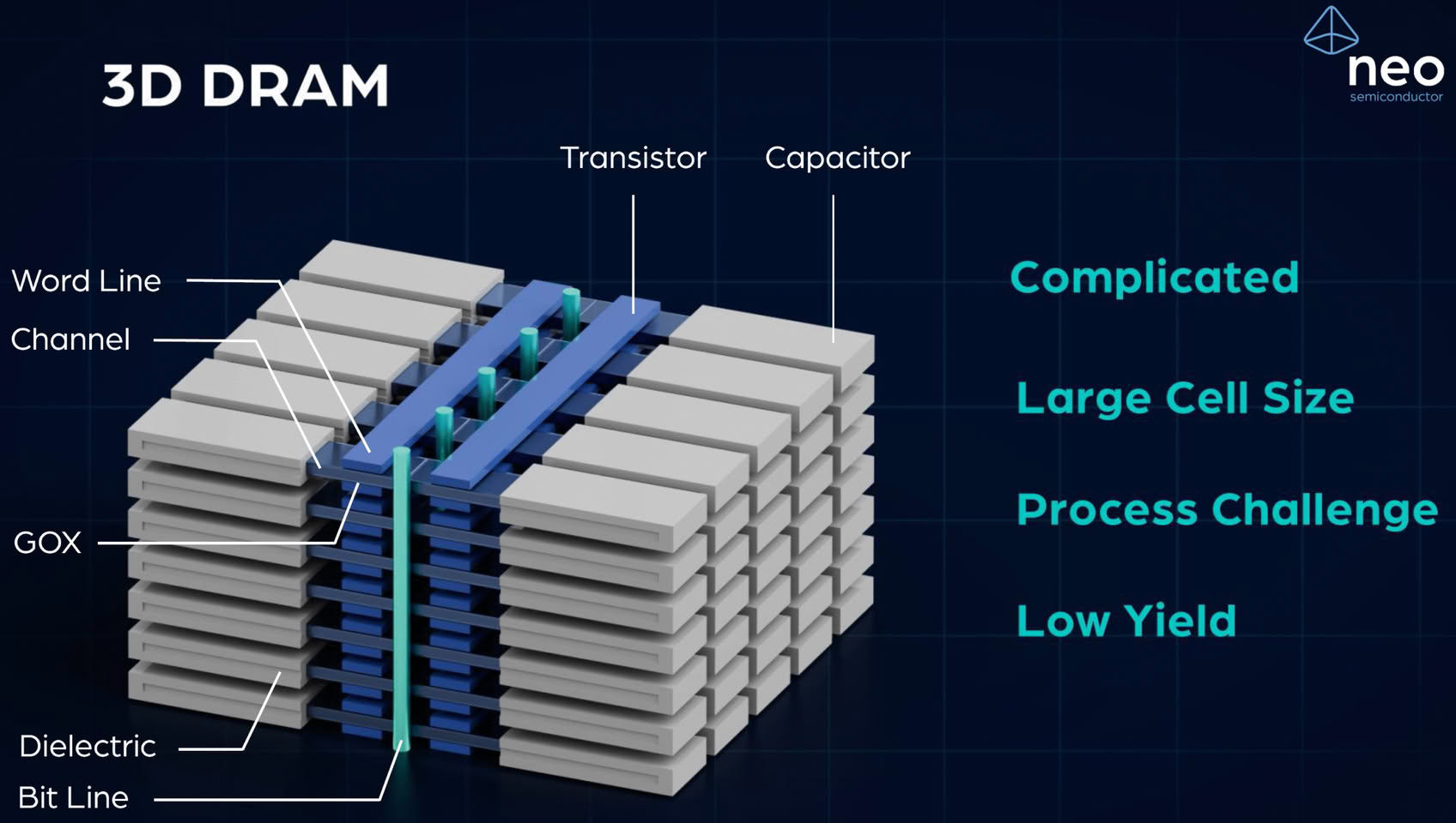
The world's largest chipmaker, TSMC, is reportedly considering entering the memory sector with the manufacturing of advanced DRAM technologies. According to a report from The Information, which cites sources close to the plans, TSMC is contemplating starting the production of 3D DRAM. As we know, there is a desperate need for more DRAM output from the three major memory makers: SK Hynix, Samsung, and Micron. New manufacturing capacity is being developed, but even when it comes online, there might still be a supply imbalance. According to The Information, TSMC is considering 3D DRAM manufacturing at the request of its largest customer, NVIDIA.

Conventional DRAM is currently produced by the big three, with plans to advance into 3D DRAM production beyond what HBM currently offers. To effectively scale memory, the 3D approach is the only way forward, as Micron recently confirmed. Micron has decided not to bring 4F² DRAM to market, even though it claims to have invented the cell design and has been researching it for around two decades, opting instead for the path to 3D DRAM. As one of the most experienced silicon manufacturers globally, TSMC is seemingly evaluating this path as well.

GlobalFoundries Reports Third Quarter 2026 Financial Results

GLOBALFOUNDRIES Inc. (GF) (Nasdaq: GFS) today announced preliminary financial results for the third quarter ended September 30, 2026.

Key Third Quarter Financial Highlights
  • Revenue of $1.899 billion
  • Gross margin of 30.1% and Non-IFRS gross margin of 31.4%
  • Operating margin of 12.1% and Non-IFRS operating margin of 17.9%
  • Net income (loss) of $(270) million and Non-IFRS net income of $298 million
  • Diluted earnings (loss) per share ("EPS") of $(0.49) and Non-IFRS EPS of $0.53
  • Non-IFRS adjusted EBITDA of $647 million
  • Ending cash, cash equivalents and marketable securities of $3.2 billion
  • Net cash provided by operating activities of $341 million and Non-IFRS adjusted free cash flow of $136 million

TSMC Could Charge Up to 20% More for CoWoS Packaging Amid AI Crunch

TSMC is reportedly considering raising prices for its CoWoS (Chip on Wafer on Substrate) advanced packaging by as much as 20%, according to supply chain sources cited by Taiwan's Commercial Times. Foundries and outsourced packaging firms are apparently weighing another round of 10% to 20% increases, as CoWoS demand has spread beyond AI GPUs to server CPUs and custom ASICs, leaving a growing backlog of unfilled orders. TSMC hasn't confirmed anything yet.

Testing is turning into a bottleneck of its own. Nomura estimates, via Seoul Economic Daily, that NVIDIA's Blackwell takes roughly four times longer than Hopper in final testing, while Rubin could need seven times as long. Packages keep growing too, with TSMC already mass producing CoWoS-L at 5.5 times the reticle limit. Tool lead times have reportedly stretched from three to six months to as long as eight months. TSMC, which usually negotiates for discounts or extra features, apparently placed this year's equipment orders at existing prices instead, which says a lot about how tight things are.

Samsung Foundry to Manufacture Anthropic AI ASIC on 2 nm Node

Samsung Foundry may be on the verge of securing a significant deal with AI lab Anthropic to manufacture AI accelerators. According to the latest report, Anthropic is developing its custom AI accelerator on Samsung's SF2 2 nm node, which will initially be produced in a lower volume of around 200,000 chips. The design and implementation of this ASIC are being handled by Broadcom, targeting around 4,000 TOPS of INT8 compute, with a TDP of 1,300 W per chip. This will be supported by either 192 GB of HBM3E or even 288 GB of HBM3E, if the design allows. The current production volume is low, as ASIC projects are typically counted in millions of chips. However, Anthropic is likely evaluating the project's viability, which requires a complete custom infrastructure with networking, rack design, power supply, cooling, and many other factors.

The current Samsung SF2 node is built using Low-NA EUV lithography and is manufactured in South Korea, with a new facility soon to be established in Taylor, Texas. For packaging these chips and integrating them with HBM, Samsung is likely to employ its I-Cube technology, which rivals TSMC's CoWoS and allows for 2.5D packaging. Combined with the 2 nm dies, Samsung can position itself as a serious manufacturing plant for external customers and slightly close the gap with TSMC and its contract manufacturing business.

AMD CEO Lisa Su Says 2027 Will Bring a "Substantial" Supply Increase

AMD will "substantially" increase its chip supply in 2027, CEO Lisa Su told reporters in Taipei on Tuesday, while admitting that demand is still running ahead of what the company can ship. Su is on her third trip to Taiwan this year, meeting partners such as Foxconn, Quanta, Acer, and ASUS, with TSMC also on the schedule. She is reportedly heading to South Korea later this week to sit down with memory suppliers Samsung and SK Hynix. Here's what she said:
We've been able to increase our supply as we've gone through 2026, and we're going to substantially increase our supply in 2027, but we can definitely use more. There's very, very high demand for the next several years. We can see very high demand, and so we need more advanced wafer capacity.

AI Chip Packaging Pushes Beyond Reticle Limits, with CoWoS-L Set to Remain the Mainstream Advanced Packaging Solution Through 2028

TrendForce's latest research into advanced semiconductor packaging reveals that GPU suppliers and hyperscale CSPs are continuing to develop increasingly powerful and versatile AI chips, making larger package sizes a key development priority for 2.5D packaging. Although TSMC's CoWoS-L faces competition from Intel's EMIB-T, its advantages in technology maturity and yield are expected to keep it the mainstream packaging solution for AI chips through 2028.

TrendForce notes that strong AI demand continues to support NVIDIA's push toward integrated GB/VR rack-scale solutions, which incorporate large numbers of chips. NVIDIA's high-end GPU shipments are expected to grow approximately 30% YoY in 2026. AMD, meanwhile, is aggressively promoting its MI400/MI450 series beginning in the second half of 2026, providing further momentum to overall shipments.

TSMC Delays Hybrid Bonding Investment for HBM, Opts for Microbumps

According to the latest report from ETNews, citing supply chain sources, TSMC is reportedly still holding back from investing in the silicon packaging technology known as hybrid bonding for HBM memory integration. For those unfamiliar, hybrid bonding creates a permanent bond between two silicon chips using embedded metal bumps that are fused together to form a single chip. Multiple dies or entire silicon wafers can be connected by stacking the back ends of two chips together. This technology eliminates traditional chip bumps and directly bonds copper interconnections between the two chips. In modern packaging, chip solder bumps, which stick out before the chip is soldered to the PCB, are roughly 100 micrometers in size, while microbumps are approximately 20 micrometers. Hybrid bonding reduces this size to 1 micrometer. Microbumps are used to interconnect silicon with other chips inside a package, as seen in CoWoS-S and CoWoS-L, where microbumps are prevalent for chip-to-interposer connections.

For TSMC, the future may involve bypassing hybrid bonding technology for packaging HBM memory and investing in microbumps that are 5 micrometers in size. Reportedly, TSMC is preparing its supply chain for 5-micrometer microbumps, which will be even smaller than what is currently available, to enhance performance in packaging. South Korean and Japanese suppliers are reportedly collaborating with TSMC to achieve this, with mass production of 5-micrometer microbumps expected in the second half of 2028. As a reminder, AMD's 3D V-Cache technology uses hybrid bonding to put SRAM on top of logic, but TSMC reportedly plans to keep integration of HBM memory into packaging on microbumps for now.

NVIDIA's "Rubin CPX" GPU Reborn with HBM4 Memory, No More GDDR7

NVIDIA has reportedly revived its "Rubin CPX" AI accelerator project, which had previously been put on hold. Today, well-known supply chain analyst Ming Chi Kuo reported that NVIDIA is reintroducing the "Rubin CPX," now featuring HBM4 memory instead of the previously planned GDDR7. Late last year, NVIDIA announced its plans to develop a specialized accelerator derived from the "Rubin" GPU family, designed for large-scale agentic AI workloads. After the announcement, the project was reportedly paused, but NVIDIA has now redesigned the memory architecture. Previously, the "Rubin CPX" was slated to have 128 GB of GDDR7 memory, but it will now include 168 GB of HBM4 memory. This GPU SKU is housed in a separate rack with configurations ranging from 64 to 256 standalone CPX GPUs per rack.

This GPU is dedicated to prefill workloads, powering racks that manage input context for LLMs and KV cache processing. Essentially, NVIDIA is separating prefill from decode tasks, with CPX GPUs handling prefill and regular "Rubin" GPUs managing decode. A rack tray with eight CPX GPUs can handle 1.34 TB of long-context prefill and the associated KV cache, all utilizing HBM4 memory for faster processing and increased bandwidth. Since the previous design did not require HBM4 integration, NVIDIA has redesigned the package, likely using TSMC's CoWoS-S or CoWoS-L for packaging.

Rapidus Targets 8-Reticle Interposers on 600 mm Advanced Packaging Panels by 2030

Rapidus has laid out its advanced packaging roadmap at the 2026 OCP APAC Summit, with eight-reticle-size interposers and 600 x 600 mm panel-level processing as the targets for around 2030. The roadmap was presented by Rapidus Design Solutions CTO Rozalia Beica and shows steps through interposer sizes from four reticles (3,320 mm²) to six (4,980 mm²) and eventually eight (6,640 mm²) by 2030. The 600 x 600 mm panel format is the most important target of that plan as the yield advantage at panel scale is substantial. CTO Beica illustrated the output difference in a simple manner: an eight-reticle interposer yields four units on a standard 300 mm wafer, nine on a 300 x 300 mm panel, 36 on a 510 x 515 mm panel, and 49 on a 600 x 600 mm panel. Taiwanese rival TSMC has its own CoWoS interposer roadmap showing plans aiming for 5.5 reticles in 2026, 9.5 in 2027, and 14 reticles in 2028. However, the two companies are taking different manufacturing approaches. Rapidus is betting on panel-level processing rather than wafer-based scaling.

The 600 mm panel strategy is underway, with Rapidus demonstrating the format and working with Lam Research's Kallisto electroplating system to develop 2.xD packaging with redistribution layers formed on 600 mm glass carriers. We reported in late 2025 that Rapidus produced the first large-format glass interposer prototype and plans to enter mass production in 2028. Last year, Rapidus taped out a 2 nm GAA test chip using ASML EUV tools claiming a transistor density of 237 MTr/mm². Its FY2026 plan brings the Rapidus Chiplet Solutions pilot line into full operation to verify 2.xD and 3D packaging processes.

NVIDIA Secures TSMC A16 Node for Next-Generation "Feynman" GPUs

According to supply chain sources and those close to TSMC, NVIDIA is already working on prototyping the replacement for its "Rubin" and "Rubin Ultra" GPU designs with the next-generation "Feynman" GPU microarchitecture. As noted in the latest report from DigiTimes, NVIDIA is opting for TSMC's A16 node, bypassing the N2 family of nodes entirely in favor of the more advanced 1.6 nm A16 design. Mass production is scheduled for the second half of 2028. The "Feynman" designs will rely on the backside power delivery in the A16 node, as well as on packaging technologies like 3D chiplets using SoIC, CoWoS-L 2.5D integration, and next-generation panel-level packaging.

Initially, NVIDIA will use SoIC 3D stacking technology to stack multiple chiplets into a single package, which will shorten the travel time between chips and reduce latency. These 3D chips will then be packaged side-by-side in a CoWoS-L or CoPoS packaging, creating a multi-kilowatt design capable of processing dozens of PetaFLOPS. For memory, NVIDIA will work with its partners to develop customized HBM, likely HBM4E, by the time "Feynman" reaches mass production. This customized memory includes a specialized base die that can contain logic elements like a memory controller or packet processing unit. Think of it as a way to pre-process data before it enters memory, or as a simple speedup, depending on what NVIDIA aims to achieve.

TSMC Achieves 98% Yield on CoWoS-L with 5.5x Reticle Size, 14x Comes in 2029

TSMC has reportedly achieved near-perfect packaging yields, establishing a baseline of about 98% for its current CoWoS advanced packaging. This technology accommodates a die area equivalent to 5.5 times the reticle limit, or about 858 mm². As a result, packaging 4,720 mm² worth of silicon on CoWoS-L is now possible, with only 1-2% of the packaged designs experiencing issues. This is a significant achievement for a packaging technology that went into mass production earlier this year. Although CoWoS-L has been shipping for some time, this year marks the first time a 5.5x reticle chip has been packaged on a mass production scale.

The Taiwanese manufacturing giant is also preparing for even larger designs, including up to 14x reticle size dies on a single, enormous package. This means a silicon area of 12,012 mm² will be packaged using TSMC's CoWoS, or specifically one of its variants. This technology is slated for 2029, when its A13 node is expected to be in mass production. TSMC's timelines are consistently being met with customer satisfaction, and the company continues to sell out its manufacturing and advanced packaging technologies. However, creating any design beyond the 3x reticle limit must be done carefully, as thermal warping can introduce mechanical issues. The company is constantly working with customers to overcome these challenges.

Intel's EMIB-T to Rival TSMC's CoWoS with 50% Cost Advantage, Volume Production in 2027

Intel's push for advanced packaging is reportedly attracting significant attention from external customers to Intel Foundry. However, the company's latest packaging will only begin mass production next year. Intel's Embedded Multi-die Interconnect Bridge (EMIB) enables designers to use 2D, 2.5D, and 3D building blocks to optimize cost, power, and bandwidth at the system level. EMIB is a substrate-embedded silicon bridge that provides localized, high-density die-to-die routing without the cost and area penalty of a full-size silicon interposer. For example, small silicon EMIB bridges—available in variants like EMIB-M with embedded MIM capacitors and EMIB-T with TSVs—offer low-cost, high-density shoreline connections ideal for logic-to-logic and logic-to-HBM interfaces. The EMIB-T variant, which includes TSVs, allows ASICs to gain direct access to power connections, resulting in a massive, multi-kilowatt solution on a single package.

However, this EMIB-T advanced packaging will only enter mass production next year, as Intel is currently ramping up its regular EMIB and Foveros for customers. According to Taiwan's Unimicron, which manufactures PCBs and silicon substrates, Intel's EMIB-T will reach high-volume production in 2027. The company also notes that customers, including ASIC designers like Broadcom and Meta, are considering switching from TSMC's CoWoS packaging to EMIB to reduce costs while maintaining the same benefits and even gaining more features in some areas. The price gap between EMIB-T and CoWoS (presumably CoWoS-L or CoWoS-R) can be as much as 50%, depending on whether an expensive interposer is required. This means that the costs of advanced packaging are passed back to the customer, who can then invest in other production areas.

TSMC Develops EMIB-like Technology to Compete with Intel

TSMC is reportedly developing an advanced packaging technology to rival Intel's Embedded Multi-die Interconnect Bridge (EMIB), which the company internally refers to as EMIB-like. According to sources close to The Information, TSMC's Chip-on-Wafer-on-Substrate (CoWoS) packaging might lose some customers to Intel's EMIB. As a result, TSMC has begun developing its EMIB-like technology. This development will reportedly be supported by Taiwan's Kinsus Interconnect Technology, which will assist TSMC in developing, scaling, and manufacturing the CoWoS alternative without issues. TSMC currently offers three versions of CoWoS: CoWoS-S, CoWoS-L, and CoWoS-R.

CoWoS-S is the first generation of CoWoS, utilizing a full monolithic silicon interposer with TSVs for maximum routing density and performance. Then, there is CoWoS-L that takes a hybrid approach, replacing the full silicon sheet with a more affordable organic base and embedding small localized silicon bridges (LSI) only where high-speed die-to-die communication occurs. This allows for large layouts to bypass reticle limits through bridge stitching. CoWoS-R is the third option that completely replaces silicon with an organic copper/polymer RDL interposer. It experiences a slight reduction in signal attenuation and routing density, but its mechanical flexibility makes it highly scalable and cost-effective for large-die chips.

TSMC Achieves Record $13.75 Billion Revenue in June 2026

TSMC's revenue reached an impressive 442.68 billion NTD in June 2026, which is about 13.75 billion USD (at the time of writing) for a single month of net revenue. This represents a remarkable 67.9% growth compared to the same month last year, driven by the record AI data center expansion. Month over month, TSMC's revenue increased by 6.2% from May 2026. These figures are impressive, considering that such high double-digit growth for a company already generating billions in revenue is one of the best performances in modern history. Additionally, TSMC generated revenue of 2,404.48 billion NTD, equivalent to about 74.66 billion USD, in the first six months of the year. This marks an increase of 35.6% compared to the first half of 2025, indicating that the trend is expected to continue.

In June, TSMC successfully began high-volume manufacturing of the N2 process. AMD has partnered with TSMC to manufacture its EPYC "Venice" on the 2 nm N2 process, alongside the CoWoS packaging that TSMC's facilities offer. AMD is now a top-tier client at TSMC, utilizing the latest nodes that were typically adopted first by Apple, followed by others. Apple is following AMD with its A20 SoC for iPhones and M6 SoC for MacBooks. TSMC's revenue target for the full year 2026 is expected to significantly surpass the 2025 figures, as the company encourages customers to adopt more advanced built on pricier wafers.

AMD Announces Production Ramp of Next-Generation AMD EPYC Processor "Venice" on TSMC 2nm Process Technology

AMD today announced that its next-generation AMD EPYC processor, codenamed "Venice," is ramping production in Taiwan on TSMC's advanced 2 nm process technology, with future plans to ramp production at TSMC's Arizona fabrication facility. The milestone in the execution of the AMD data center CPU roadmap demonstrates continued progress toward delivering the leadership performance and energy efficiency required for next-generation cloud, enterprise and AI infrastructure. "Venice" is the first high-performance computing (HPC) product in the industry to enter production on TSMC's advanced 2 nm process technology.

"Ramping 'Venice' on TSMC 2 nm process technology marks an important step forward in accelerating the next generation of AI infrastructure," said Dr. Lisa Su, chair and CEO, AMD. "As AI and agentic workloads scale rapidly, customers need platforms that can move from innovation to production faster. Our deep partnership with TSMC is helping AMD bring leadership compute technologies to market with the speed and scale required to meet this moment."

SK hynix Eyes Intel EMIB 2.5D Packaging for HBM Memory

SK hynix is collaborating with Intel to utilize its Embedded Multi-die Interconnect Bridge (EMIB) 2.5D packaging technology for HBM memory. As SK hynix aims to diversify its supply chain and customers are increasingly considering Intel Foundry, the South Korean memory giant is exploring research and development efforts with Intel on 2.5D packaging technology. Intel's premier 2.5D packaging technology is its EMIB, which interconnects multiple silicon dies using bridges embedded in a packaging substrate. SK hynix is interested in integrating this technology into its HBM memory, presumably to bring its HBM4 memory modules up to standard for EMIB integration, should its AI chip partners choose Intel Foundry for advanced packaging of their next-generation solutions.

We have already covered that small silicon EMIB bridges—available in variants like EMIB-M with embedded MIM capacitors and EMIB-T with TSVs—provide low-cost, high-density shoreline connections ideal for logic-to-logic and logic-to-HBM interfaces. However, until now, SK hynix has been using TSMC and its CoWoS 2.5D packaging technology. As CoWoS is gradually reaching its limits and customers are seeking alternative packaging methods, EMIB is emerging as a strong candidate to continue the scaling of chiplets in many directions beyond the traditional reticle limit of 830 mm² of silicon area.

TSMC Debuts A13 Technology at 2026 North America Technology Symposium

TSMC (TWSE: 2330, NYSE: TSM) today debuted its latest innovation in its most advanced process technology at the Company's 2026 North America Technology Symposium. TSMC's new A13 process is a direct shrink of its industry-leading A14 node announced in 2025, enabling even more compact and efficient designs to address insatiable customer demand in computational requirements for next-generation artificial intelligence, high performance computing (HPC), and mobile applications.

Representing TSMC's commitment to continuous improvement, A13 provides 6% area savings from A14. Design rules are fully backward compatible with A14, enabling customers to quickly migrate their designs to TSMC's latest nanosheet transistor technology. In addition, A13 delivers increased power efficiency and performance gains through design-technology co-optimization, and is scheduled to enter production in 2029, one year after A14.

Intel Foundry Nears Major Customer Wins as Apple, AMD, Google, and NVIDIA Weigh Deals

Intel Foundry has been attracting significant attention from the industry lately, with some of the world's largest companies expected to announce new foundry commitments this fall, according to UBS Group. The investment bank has reported that Intel Foundry is on the brink of securing many new contracts scheduled for this fall, citing the release of version 1.0 of the 14A node process design kit (PDK) as a key catalyst. There have been numerous rumors that Apple, AMD, NVIDIA, Google, and Broadcom are considering utilizing Intel's silicon manufacturing, including the 18A, 18A-P, and 18A-PT nodes, as well as the upcoming 14A node. Apple is rumored to manufacture some of its M-Series "Apple Silicon" laptop processors in 2027 using the 18A-P node, while Google might leverage Intel's EMIB and Foveros 3D advanced packaging technology for some of its TPU designs.

Companies regularly evaluate leading industry nodes but often choose TSMC's manufacturing due to its reliability, high volume capacity, and advanced packaging, which has produced numerous high-performance and low-power designs at scale. However, Intel Foundry has been investing significant resources and logistics into attracting external clients, leading UBS to anticipate multiple foundry commitments being announced this fall. Late last year, we learned that Apple was waiting for Intel to release the 18A-P PDK version 1.0 or 1.1, scheduled for Q1 and Q2 of 2026, respectively. As we are now in Q2, we are awaiting further confirmation to see if Apple proceeded with the deal, but UBS expects it did.

NVIDIA's "Rubin Ultra" Reportedly Faces Issues With CoWoS-L Packaging

NVIDIA is reportedly experiencing manufacturing issues with its next-generation "Rubin Ultra" GPU design, one of the company's most ambitious chip development projects, due to the limitations of modern packaging technology. The world's largest company is already shipping customer samples of the standard "Rubin" GPUs, with mass shipments set to begin this summer. However, the current roadmap for the upgraded "Rubin Ultra" design may be encountering technological limitations, as NVIDIA's design goals are too ambitious for TSMC's packaging capabilities. Reportedly, NVIDIA plans to double the regular "Rubin" two-die package with 8 HBM4 modules into a new "Rubin Ultra" package that will include four silicon dies and 16 HBM4E modules in a single package. This configuration is scheduled for 2027, but the sheer volume of silicon may be too much for TSMC's packaging, according to Global Semi Research.

In a typical CoWoS package, TSMC usually combines multiple smaller dies and multiple HBM memory modules into a unified package that supports the entire AI build-out. However, with the ambitious "Rubin Ultra" design, NVIDIA planned to use CoWoS-L, which was expected to handle the design and concept that "Rubin Ultra" was based on. It is rumored, however, that in a 2+2 die package—meaning four dies as in this architecture—TSMC is encountering warping issues. The package—which includes a substrate—is bending in multiple directions, causing the compute dies of "Rubin Ultra" to not make complete contact with the underlying substrate. This instability means that TSMC has to explore alternatives within its packaging portfolio. One of these alternatives is a panelized approach called CoPoS, which stands for Chip-on-Panel-on-Substrate.

NVIDIA Stops China-Focused H200 "Hopper" GPU Production

NVIDIA has reportedly halted production of its China-focused H200 "Hopper" GPU at TSMC's facilities, according to multiple reports. The company has built up an inventory of 250,000 H200 GPUs, which will be available in the Chinese market for select applications that do not compromise United States national security. After NVIDIA was granted export rights to China for its H200 accelerators, the company began stockpiling these GPUs to supply AI labs across China. However, China has also restricted what its domestic companies and AI labs can import, meaning that the import of H200 GPUs is still prohibited unless a company receives a letter of exemption from Beijing. This has resulted in NVIDIA using its TSMC N5 5 nm node capacity to create about 250,000 units, which are now stored in a warehouse awaiting export approval from the U.S. administration and import approval from Chinese customs for AI labs.

Interestingly, the Financial Times and Reuters note that NVIDIA will now "reallocate" capacity from H200 production to the new "Rubin." However, these two GPU generations do not use the same manufacturing node or packaging technology. For "Hopper," NVIDIA uses TSMC's 5 nm node with CoWoS-S packaging, while "Rubin" uses a 3 nm node with CoWoS-L packaging. These reports likely refer to some conversion of manufacturing capacity involving either the node or packaging capacity that NVIDIA has secured. It is unlikely that the 5 nm semiconductor node can be converted into a 3 nm node without significant line remodeling and changes to manufacturing equipment. However, packaging can be adjusted more easily, which is likely what these reports are indicating.

Amkor to Significantly Boost Arizona Packaging Capacity for Intel and TSMC

Amkor is preparing to greatly expand its Arizona-based operations, and the company will boost its spending not by a few percent, but by several multiples. The company is planning to triple its capital expenditures next year, with a dramatic increase from roughly $900 million in 2025 to as much as $3 billion in 2026, betting on massive demand from Intel and TSMC packaging technologies. This includes working with Intel and TSMC to enable their most advanced technologies like EMIB and CoWoS, all of which come in various form factors. We previously reported that Intel partnered with its long-time OSAT partner Amkor to take additional EMIB capacity that Intel's customers are interested in, in Incheon, South Korea.

However, as Amkor expands its facilities in Arizona, Intel will also collaborate with Amkor to deliver advanced EMIB packaging types on United States soil. While TSMC has been a primary choice for many high-density assemblies, growing interest in Intel's EMIB and Foveros options has led partners like MediaTek, Google, Qualcomm, and Tesla to consider alternatives. Interestingly, Amkor will also offload some of the CoWoS packaging work from TSMC by creating CoWoS packages on U.S. soil, instead of sending these chips back to TSMC's Taiwan fabs to finish production. Both CoWoS and EMIB/Foveros offer a list of benefits, making them highly sought-after packaging technologies for companies seeking to extract maximum performance from their chips. Amkor plans to be at the center of that supply chain and help Intel and TSMC handle more customers.

Samsung's Texas Fab Reportedly Attracting Major Customer Interest as AI Boom Continues

A report put together by Deutsche Bank analysts has mentioned an ongoing supply-demand imbalance within the semiconductor market. According to Jukan's summary of the financial institute's findings, TSMC's "share of the advanced-node foundry market" could fall from an impressive 95% level, down to a mere 90% in the coming years. The industry-leading chipmaker continues to enjoy a prime position, but its international operation footprint seemingly cannot keep up with requests—mainly from fabless customers—during the ongoing AI hardware boom. Deutsche Bank believes that the Taiwanese foundry business has an order backlog extending way into 2027, with many clients requiring 3 nm wafer products. TSMC reportedly aims to get 3 nm node production lines pumping out around 190,000 wafers per month, by the end of this year. Even if this major target is met, demand is expected to outweigh supply. AI chip production-centric bottlenecks—mostly involving CoWoS packaging—have been dealt with in the recent past, but industry observers posit that VIP customers are considering alternate providers.

Allegedly, the next best options are the Samsung and Intel Foundries, despite rumors of teething problems—both companies will very likely welcome new requests. In modern times, many of Samsung's big clients have switched over to TSMC, due to (the former's) supposedly troubled development of more advanced nodes. Deutsche Bank analysts have outlined a "big six" group of key customers: AMD, Apple, Broadcom, MediaTek, NVIDIA, and Qualcomm. The fabless firms could be pursuing alternate "production capacity" avenues, with Samsung's 2 nm (SF2) and 4 nm node process lines being of particular interest. Like TSMC, the South Korea megacorp's state-of-the-art fabrication sites and staff expertise are concentrated in home territories. A surprise prediction has highlighted Samsung's main North American foundry—the Deutsche Bank report pinpointed a very specific location: "for customers seeking alternative supply, Samsung's Taylor fab is more likely to become the first destination." In addition, analysts think that the big six will select Samsung's Texas-based foundry over Intel's best native site (perhaps dealing in 18A).

Intel Envisions 16 Compute Dies and 24 HBM5 Modules in a Single Package

Intel Foundry has published a short video demonstration of its advanced packaging technologies, demoing silicon scaling beyond reticle limits of 830 mm². According to the video, Intel's Foveros 3D and EMIB-T interconnect can scale silicon to 12x reticle size, packaging up to 16 compute dies paired with 24 HBM5 memory modules in a single package. All of this will leverage Intel's 18A—including 18A-P and 18A-PT—and 14A nodes that the company is preparing for mass production and external customers.

The approach involves a sophisticated layering technique where base dies, manufactured using the 18A-PT process, incorporate backside power delivery to enhance logic density and reliability. These base dies house SRAM structures similar to Intel's "Clearwater Forest" architecture. They serve as foundations for compute tiles built on the advanced 14A/14A-E nodes, which feature second-generation RibbonFET transistors and PowerDirect technology. Foveros Direct 3D enables vertical stacking through ultra-fine pitch hybrid bonding, while EMIB-T incorporates through-silicon vias to facilitate higher bandwidth connections between chiplets. This combination achieves scalability beyond reticle limits and will support all HBM standard, including HBM4, HBM5, and future versions.

NVIDIA and AMD Explore Intel 14A Node, Apple and Broadcom Considering Intel EMIB Packaging

NVIDIA and AMD are reportedly evaluating Intel Foundry's 14A node, while Apple and Broadcom are considering Intel's EMIB packaging for a custom server accelerator. According to GF Securities Hong Kong, these developments reflect a growing willingness among top designers to reconsider their sources for both front-end process technology and back-end assembly. Capacity limits at alternative suppliers like TSMC are likely a key factor prompting these exploratory moves, with packaging availability now a central constraint for large design houses.

Closer to Apple, supply chain reports indicate the company has engaged Intel for process evaluation and is weighing alternative packaging routes. Apple has reportedly worked with version 0.9.1 of the 18A-P process design kit and is awaiting PDK 1.0 or 1.1, expected in the first quarter of 2026, before moving into larger scale tests. The Broadcom-assisted "Baltra" server design was originally linked to TSMC's N3 3 nm processes, but limited CoWoS capacity at TSMC has led Apple to consider Intel for packaging with EMIB options. At the same time, shipments of the custom AI server parts now seem more likely in 2028, while lower-end M-series chips built on Intel process technology could appear in 2027 if PDK revisions and yield targets prove sufficient for Apple.
Return to Keyword Browsing
Nov 17th, 2026 22:46 CST change timezone

New Forum Posts

Popular Reviews

TPU on YouTube

Controversial News Posts