News Posts matching #DDR5

Return to Keyword Browsing

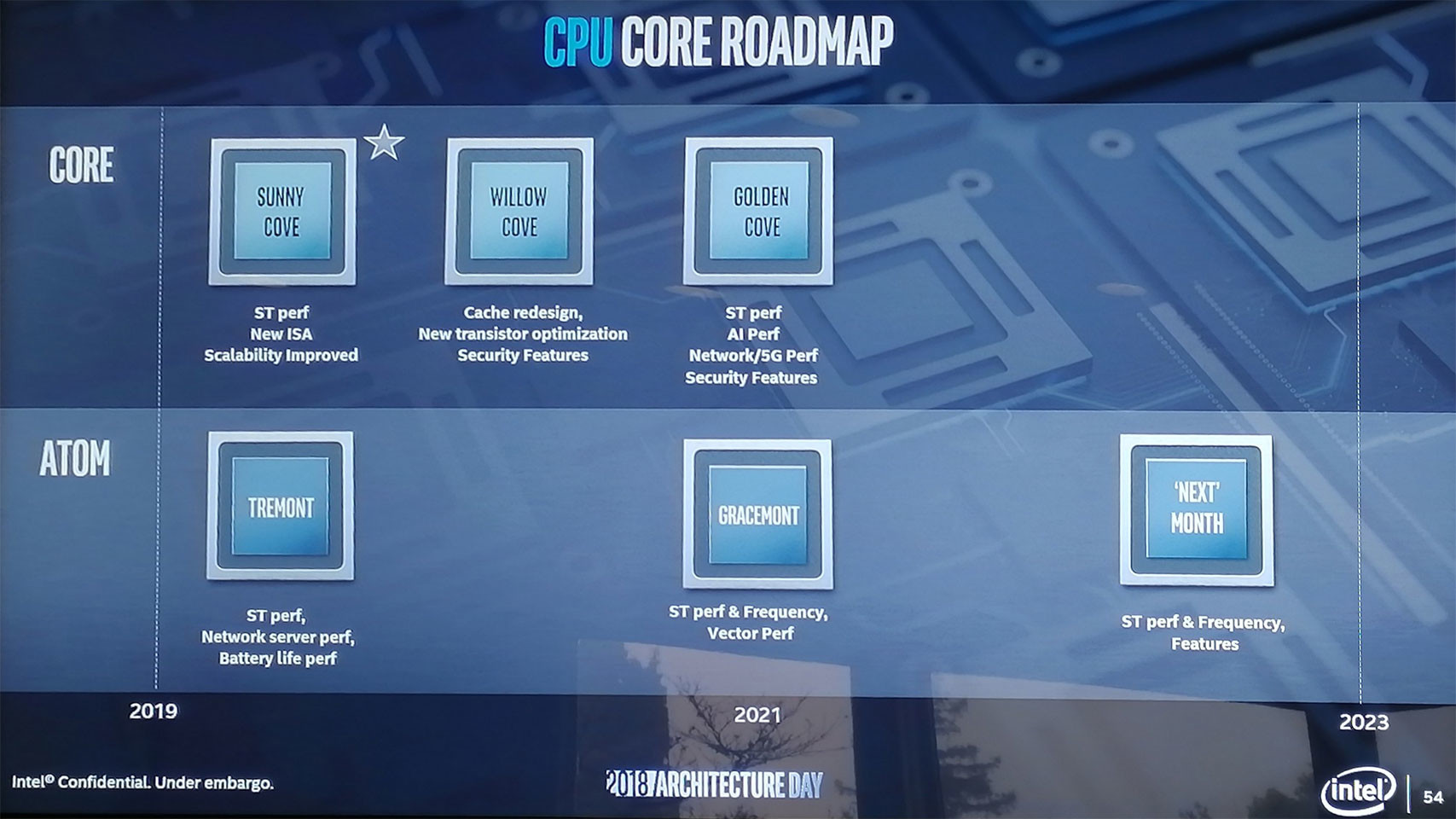
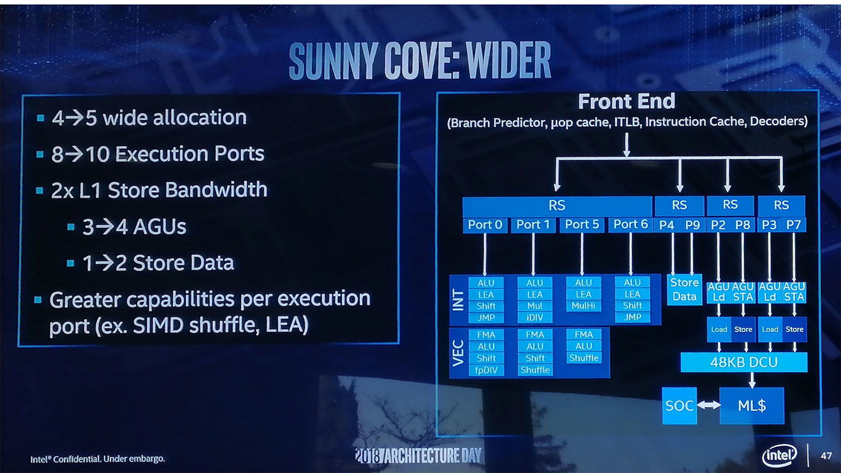
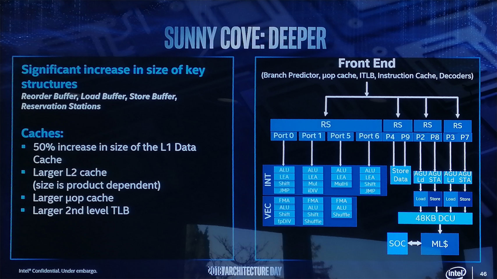
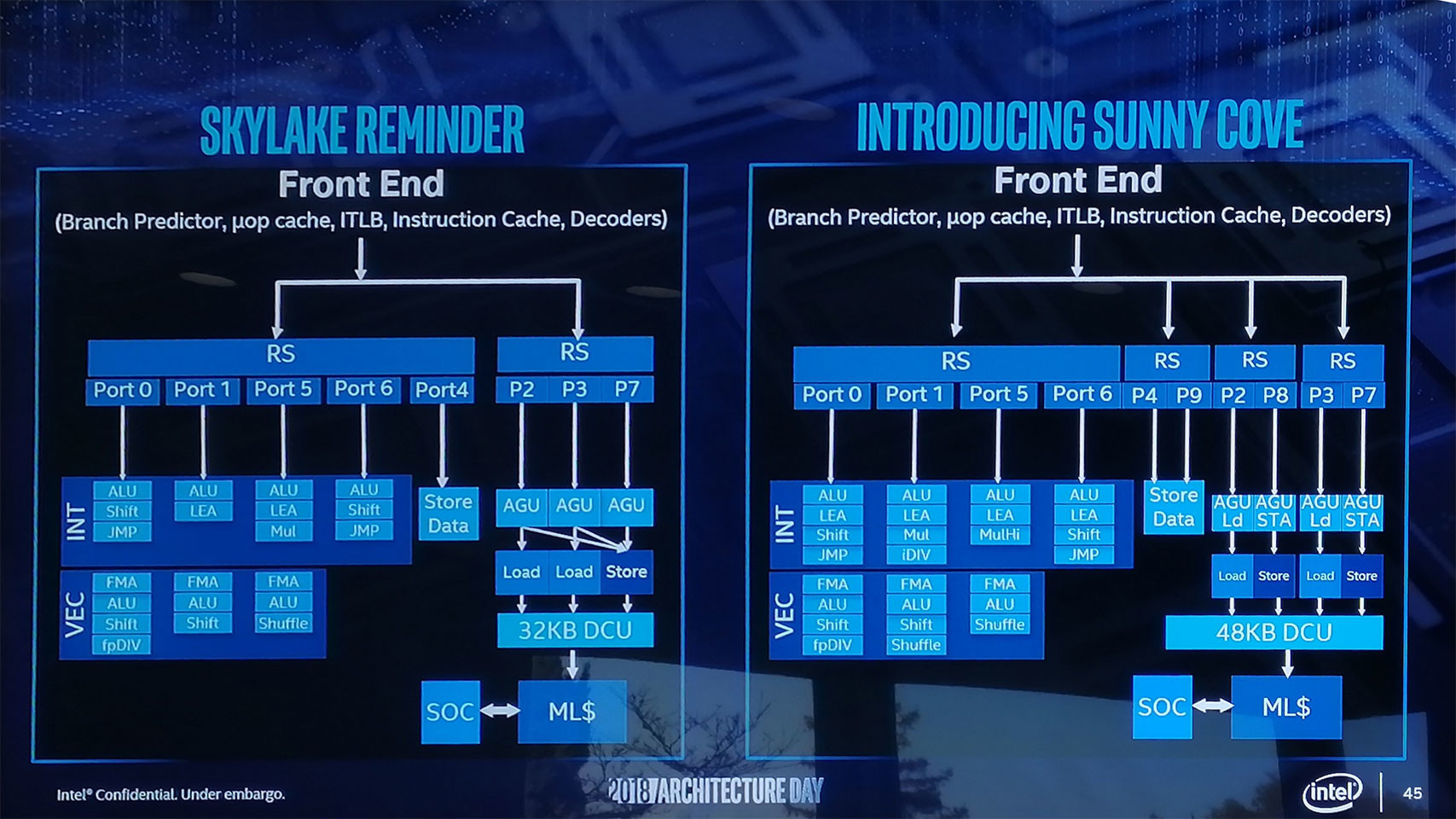
Europe Readies its First Prototype of Custom HPC Processor

European Processor Initiative (EPI) is a Europe's project to kickstart a homegrown development of custom processors tailored towards different usage models that the European Union might need. The first task of EPI is to create a custom processor for high-performance computing applications like machine learning, and the chip prototypes are already on their way. The EPI chairman of the board Jean-Marc Denis recently spoke to the Next Platform and confirmed some information regarding the processor design goals and the timeframe of launch.

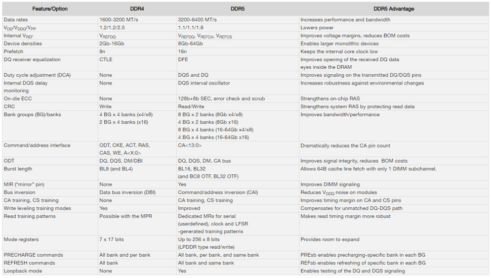
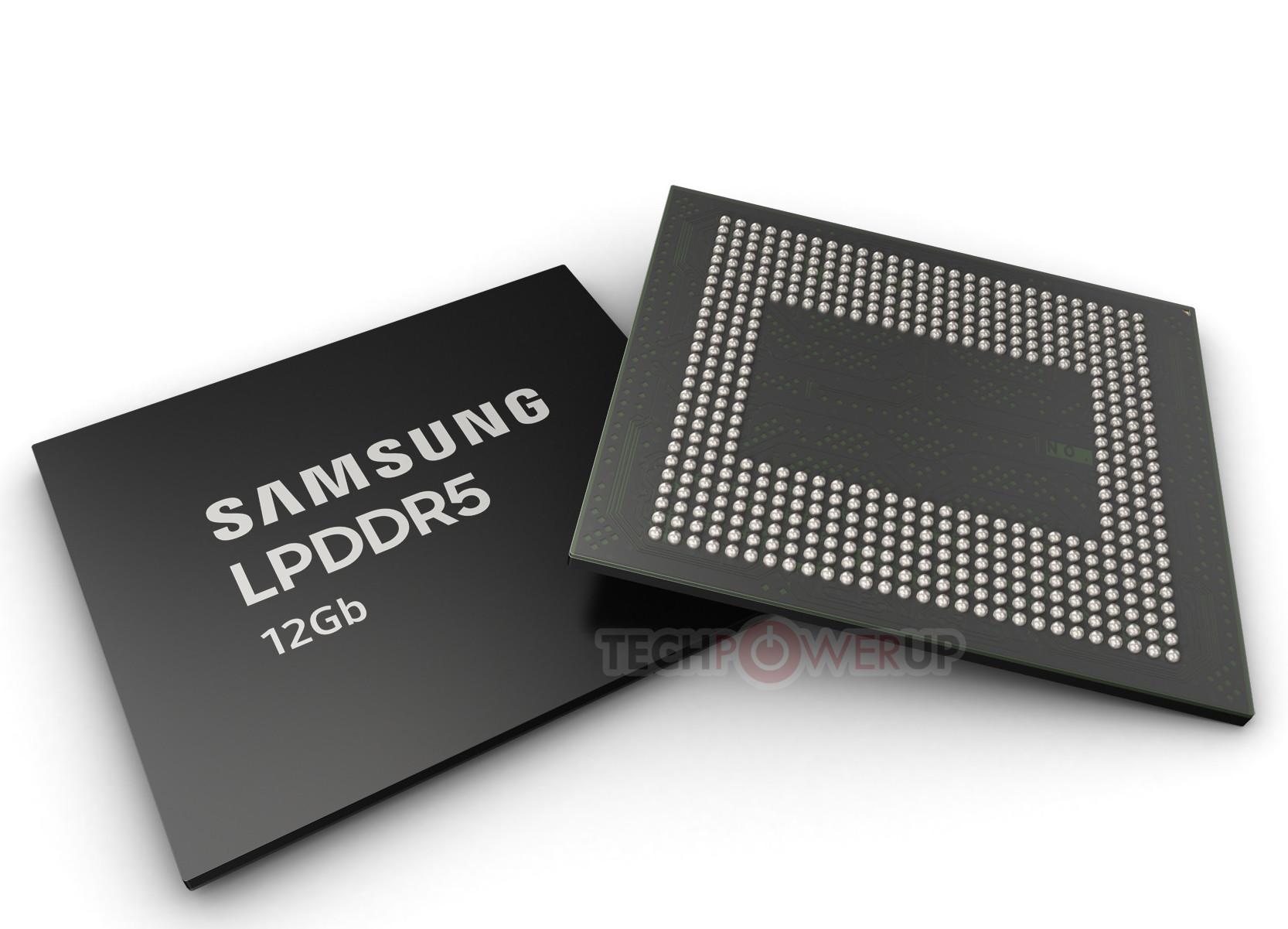
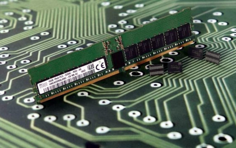
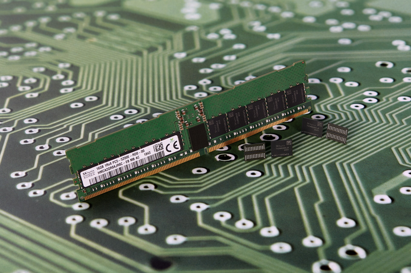
Supposed to be manufactured on TSMC's 6 nm EUV (TSMC N6 EUV) technology, the EPI processor will tape-out at the end of 2020 or the beginning of 2021, and it is going to be heterogeneous. That means that on its 2.5D die, many different IPs will be present. The processor will use a custom ARM CPU, based on a "Zeus" iteration of Neoverese server core, meant for general-purpose computation tasks like running the OS. When it comes to the special-purpose chips, EPI will incorporate a chip named Titan - a RISC-V based processor that uses vector and tensor processing units to compute AI tasks. The Titan will use every new standard for AI processing, including FP32, FP64, INT8, and bfloat16. The system will use HBM memory allocated to the Titan processor, have DDR5 links for the CPU, and feature PCIe 5.0 for the inner connection.

SK hynix Displays its Semiconductor Technologies Leading the 4th Industrial Revolution

SK hynix Inc. presents its innovative semiconductor technologies leading the 4th Industrial Revolution at CES 2020, the world's largest trade show for IT and consumer electronics in Las Vegas, USA, from January 7-10, 2020. In line with its "Memory Centric World" theme, SK hynix depicts a futuristic city which effectively utilizes enormous amounts of data. The Company also showcases its semiconductor solutions across six crucial business fields - artificial intelligence (AI), augmented reality (AR) / virtual reality (VR), automotive, Internet of Things (IoT), big data and 5G.

Headlining at CES 2020 are SK hynix's memory solutions including HBM2E, DDR5 for servers, and SSD, which are already highly regarded and widely used in 4th industrial fields such as 5G and AI for their stability, speed, power consumption and density excellence. Other cutting-edge products set to make headlines in January are the Company's highly durable LPDDR4X and eMMC 5.1, which are optimized for automobiles. What's more, SK hynix is displaying its LPDDR5 and UFS that enhance the performance of 5G smartphones as well as CIS (CMOS Image Sensor) which is essential in establishing effective environments for AR/VR and IoT.

Micron Start Sampling DDR5 RDIMMs

Micron has today announced that it started sampling RDIMMs based on DDR5 technology to its industry partners. Designed for server operations, these DDR5 modules come in RDIMM form-factor and feature Error-Correcting Code (ECC) technology for removing any error that occurs inside electronic circuits. The new DDR5 standard offers a massive performance uplift compared to the previous generation of DDR4 memory. For starters, DDR5 will double the MT/s transfer rate to 6400 MT/s, double the speed of the original 3200 MT/s speed for DDR4 that was established by JEDEC. The bandwidth of the new DDR memory is supposed to be 32 GB/s, which is 25% faster than the original 25.6 GB/s bandwidth of DDR4.

With DDR5, the SDRAM prefetch buffer data size is being doubled to 16 data words per memory access, making for a 16n prefetching throughput. Another improvement is that the highest possible density for DDR5 chips is now being up to 64 Gb per chip. Additionally, DDR5 is supposed to bring the power needed for chip operation down to 1.1 volts, which is around 8% lower than what DDR4 achieved. There are also features like MIR (Mirror Pin) which provides better DIMM signaling, and more options for PRECHARGE and REFRESH commands that can now operate on a per bank basis, so specific banks can be refreshed in bank group. It is also worth pointing out that DDR5 chips are manufactured using 1znm memory manufacturing process.

Intel "Tiger Lake-U" Processors Could Support LPDDR5 Memory

Intel's Core "Tiger Lake" microarchitecture could be a point of transition between DDR4 and DDR5 for the company. Prototypes of devices based on the ultra-compact "Tiger Lake-Y" SoC were earlier shown featuring LPDDR4X memory, although a new device, possibly a prototyping platform, in the regulatory queue with the Eurasian Economic Commission describes itself as featuring a "Tiger Lake-U" chip meant for thin and light notebooks and convertibles. This device features newer LPDDR5 memory, according to its regulatory filing.

LPDDR5 succeeds LPDDR4X as the industry's next low-power memory standard, offering data-rates of up to 6,400 MT/s (versus up to 4,266 MT/s of LPDDR4X), and consumes up to 30 percent less power. This prototype at the EEC is sure to be using unreleased LPDDR5 memory chips as DRAM majors Samsung and SK Hynix plan to ship their DDR5-based memory solutions only by the end of this year, although mass-production of the chips have already started at Samsung, in PoP form-factors. A successor to the 10th generation Core "Ice Lake," "Tiger Lake" will be Intel's second CPU microarchitecture designed for its 10 nm silicon fabrication node.

Intel Ships First 10nm Agilex FPGAs

Intel today announced that it has begun shipments of the first Intel Agilex field programmable gate arrays (FPGAs) to early access program customers. Participants in the early access program include Colorado Engineering Inc., Mantaro Networks, Microsoft and Silicom. These customers are using Agilex FPGAs to develop advanced solutions for networking, 5G and accelerated data analytics.

"The Intel Agilex FPGA product family leverages the breadth of Intel innovation and technology leadership, including architecture, packaging, process technology, developer tools and a fast path to power reduction with eASIC technology. These unmatched assets enable new levels of heterogeneous computing, system integration and processor connectivity and will be the first 10nm FPGA to provide cache-coherent and low latency connectivity to Intel Xeon processors with the upcoming Compute Express Link," said Dan McNamara, Intel senior vice president and general manager of the Networking and Custom Logic Group.

Samsung Begins Mass Production of Industry's First 12Gb LPDDR5 Mobile DRAM

Samsung Electronics, the world leader in advanced memory technology, today announced that it has begun mass producing the industry's first 12-gigabit ( Gb) LPDDR5 mobile DRAM, which has been optimized for enabling 5G and AI features in future smartphones. The new mobile memory comes just five months after announcing mass production of the 12 GB LPDDR4X, further reinforcing the company's premium memory lineup. Samsung also plans to start mass producing 12-gigabyte (GB) LPDDR5 packages later this month, each combining eight of the 12 Gb chips, in line with growing demand for higher smartphone performance and capacity from premium smartphone manufacturers.

"With mass production of the 12 Gb LPDDR5 built on Samsung's latest second-generation 10-nanometer (nm) class process, we are thrilled to be supporting the timely launch of 5G flagship smartphones for our customers worldwide," said Jung-bae Lee, executive vice president of DRAM Product & Technology, Samsung Electronics. "Samsung remains committed to rapidly introducing next-generation mobile memory technologies that deliver greater performance and higher capacity, as we continue to aggressively drive growth of the premium memory market."

Intel "Sapphire Rapids" Brings PCIe Gen 5 and DDR5 to the Data-Center

As if the mother of all ironies, prior to its effective death-sentence dealt by the U.S. Department of Commerce, Huawei's server business developed an ambitious product roadmap for its Fusion Server family, aligning with Intel's enterprise processor roadmap. It describes in great detail the key features of these processors, such as core-counts, platform, and I/O. The "Sapphire Rapids" processor will introduce the biggest I/O advancements in close to a decade, when it releases sometime in 2021.

With an unannounced CPU core-count, the "Sapphire Rapids-SP" processor will introduce DDR5 memory support to the data-center, which aims to double bandwidth and memory capacity over the DDR4 generation. The processor features an 8-channel (512-bit wide) DDR5 memory interface. The second major I/O introduction is PCI-Express gen 5.0, which not only doubles bandwidth over gen 4.0 to 32 Gbps per lane, but also comes with a constellation of data-center-relevant features that Intel is pushing out in advance as part of the CXL Interconnect. CXL and PCIe gen 5 are practically identical.

Intel Driving Data-Centric World with New 10nm Intel Agilex FPGA Family

Intel announced today a brand-new product family, the Intel Agilex FPGA. This new family of field programmable gate arrays (FPGA) will provide customized solutions to address the unique data-centric business challenges across embedded, network and data center markets. "The race to solve data-centric problems requires agile and flexible solutions that can move, store and process data efficiently. Intel Agilex FPGAs deliver customized connectivity and acceleration while delivering much needed improvements in performance and power for diverse workloads," said Dan McNamara, Intel senior vice president, Programmable Solutions Group.

Customers need solutions that can aggregate and process increasing amounts of data traffic to enable transformative applications in emerging, data-driven industries like edge computing, networking and cloud. Whether it's through edge analytics for low-latency processing, virtualized network functions to improve performance, or data center acceleration for greater efficiency, Intel Agilex FPGAs are built to deliver customized solutions for applications from the edge to the cloud. Advances in artificial intelligence (AI) analytics at the edge, network and the cloud are compelling hardware systems to cope with evolving standards, support varying AI workloads, and integrate multiple functions. Intel Agilex FPGAs provide the flexibility and agility required to meet these challenges and deliver gains in performance and power.

JEDEC Updates Standard for Low Power Memory Devices: LPDDR5

JEDEC Solid State Technology Association, the global leader in standards development for the microelectronics industry, today announced the publication of JESD209-5, Low Power Double Data Rate 5 (LPDDR5). LPDDR5 will eventually operate at an I/O rate of 6400 MT/s, 50% higher than that of the first version of LPDDR4, which will significantly boost memory speed and efficiency for a variety of applications including mobile computing devices such as smartphones, tablets, and ultra-thin notebooks. In addition, LPDDR5 offers new features designed for mission critical applications such as automotive. Developed by JEDEC's JC-42.6 Subcommittee for Low Power Memories, LPDDR5 is available for download from the JEDEC website.

With the doubling of memory throughput over the previous version of the standard (LPDDR5 is being published with a data rate of 6400 MT/s, compared to 3200 MT/s for LPDDR4 at its publication in 2014), LPDDR5 promises to have an enormous impact on the performance and capabilities of the next generation of portable electronic devices. To achieve this performance improvement, LPDDR5 architecture was redesigned; moving to 16Banks programmable architecture and multi-clocking architecture.

SuperMicro Gearing for Launch of New Gaming-Grade Motherboards With PCIe Gen4 and DDR5 Wave

SuperMicro may not be household name in consumer motherboards right now, but they once were a decent alternative in the market - or so I've been told by people much more knowledgeable than me in that regard, as I never laid my hands on one. The company is now more known for its server products, where it has focused most of its attention in the past decade - an effort that gave it a good, third-place hold in that market. And if the company can command such a market share in a much more requirements-heavy environment such as the server market demands, then it's likely those design decisions and developments will find themselves trickling down to the consumer side in any sort of consumer, gaming-grade product the company decided to tackle.

To that end, SuperMicro is gearing up to re introduce themselves to the consumer market, accompanying the wave of new technologies coming to the market in a few years - namely, PCIe Gen 4 and DDR5 memory. The company seems to think that this will mark a perfect opportunity for a strong comeback to the consumer market - where they now only offer a handful of motherboard solutions for Intel's CPUs. One such example is the C9Z390-PGW motherboard, based on Intel's Z390 chipset - with its 10-phase VRM design, PLC chip for doubling of PCIe lanes, and 10 Gigabit Lan. But not only on said "typical" consumer motherboard techonologies will SuperMicro be delivering - if the company has its way, anything from 5G, IoT, Mission Learning and Artificial Intelligence can be incorporated for some use case or another on consumer-grade motherboards, thus providing an axis of penetration for SuperMicro - and its entire partner eco-system.

SK Hynix Fellow Says PC5 DDR5 by 2020, DDR6 Development Underway

The PC5 DDR5 main memory standard could enter the market by 2020, according to SK Hynix research fellow Kim Dong-Kyun. The first such memory standard will be DDR5-5200, which offers nearly double the bandwidth of DDR4-2666. "We are discussing several concepts of the post DDR5," he said. "One concept is to maintain the current trend of speeding up the data transmission, and another is to combine the DRAM technology with system-on-chip process technologies, such as CPU," he added, without offering any additional information. SK Hynix had in 2018 developed a working prototype of a 16-gigabit (2 GB) DDR5 DRAM chip ticking at 5200 MT/s, at 1.1 Volts. A 64-bit wide memory module made with these chips could offer bandwidth of 41.6 GB/s.

SK Hynix is developing its own innovations that could make its DDR5 chips more advanced than the competition without going off-standard. "We have developed a multi-phase synchronization technology that enables keeping the voltage during a high-speed operation in a chip at a low level by placing multiple phases within the IP circuit, so the power used on each phase is low but the speed is high when combined," Kim said. He also mentioned that development of the DDR6 PC memory standard is already underway, with the design goals of doubling bandwidth and densities over DDR5. Advancements in DRAM are propelled not just by the PC ecosystem, but also handhelds and self-driving car electronics.

Intel Unveils a Clean-slate CPU Core Architecture Codenamed "Sunny Cove"

Intel today unveiled its first clean-slate CPU core micro-architecture since "Nehalem," codenamed "Sunny Cove." Over the past decade, the 9-odd generations of Core processors were based on incrementally refined descendants of "Nehalem," running all the way down to "Coffee Lake." Intel now wants a clean-slate core design, much like AMD "Zen" is a clean-slate compared to "Stars" or to a large extent even "Bulldozer." This allows Intel to introduce significant gains in IPC (single-thread performance) over the current generation. Intel's IPC growth curve over the past three micro-architectures has remained flat, and only grew single-digit percentages over the generations prior.

It's important to note here, that "Sunny Cove" is the codename for the core design. Intel's earlier codenaming was all-encompassing, covering not just cores, but also uncore, and entire dies. It's up to Intel's future chip-designers to design dies with many of these cores, a future-generation iGPU such as Gen11, and a next-generation uncore that probably integrates PCIe gen 4.0 and DDR5 memory. Intel details "Sunny Cove" as far as mentioning IPC gains, a new ISA (new instruction sets and hardware capabilities, including AVX-512), and improved scalability (ability to increase core-counts without running into latency problems).

SK Hynix Announces 1Ynm 16Gb DDR5 DRAM

SK Hynix announced that it has developed 16 Gb DDR5 DRAM, the industry's first DDR5 to meet the JEDEC standards. The same 1Ynm process technology used for the recently-developed 1Ynm 8Gb DDR4 DRAM was applied to the new DRAM, giving an industry-leading competitive edge for the Company.

DDR5 is a next-generation DRAM standard that offers ultra-high speed and high density with reduced power consumption as compared to DDR4, for use in data-intensive applications such as big data, artificial intelligence, and machine learning.

Cadence, Micron Update on DDR5: Still On Track, 1.36x Performance Increase Over DDR4 at Same Data Rate

DDR5 will be the next step in DDR5 memory tech, again bringing increased transfer speeds over the previous JEDEC (the standards body responsible for the DDR specifications) specification. The new memory technology will also bring the customary reductions in operating voltage - the new version will push the 64-bit link down to 1.1V and burst lengths to 16 bits from 1.2V and 8 bits. In addition, DDR5 lets voltage regulators ride on the memory card rather than the motherboard. CPU vendors are also expected to expand the number of DDR channels on their processors from 12 to 16, which could drive main memory sizes to 128 GB from 64 GB today.

DDR5 is being developed with particular attention to the professional environment, where ever-increasingly gargantuan amounts of addressable memory are required. One of the guiding principles over DDR5's development is a density increase (to allow 16 Gbit chips) that would allow for larger volumes of memory (and thus data processing) in the environments that need that. Reduced power consumption also plays a role here, but all of this will have a cost: latency. For end-users, though, this increased latency will be offset by the usual suspects (DDR memory companies such as Crucial, Corsair, just to name some started with the letter C) in tighter timings and increased operating frequencies. JEDEC's specification for DDR5 is set at 4800 MT/s, but it's expected the memory tech will scale to 6400 MT/s, and you know overclocking and performance-focused companies will walk all over the standard.

Samsung Announces First 8Gb LPDDR5 DRAM using 10 nm Technology

Samsung Electronics, the world leader in advanced memory technology, today announced that it has successfully developed the industry's first 10-nanometer (nm) class* 8-gigabit (Gb) LPDDR5 DRAM. Since bringing the first 8Gb LPDDR4 to mass production in 2014, Samsung has been setting the stage to transition to the LPDDR5 standard for use in upcoming 5G and Artificial Intelligence (AI)-powered mobile applications.

The newly-developed 8Gb LPDDR5 is the latest addition to Samsung's premium DRAM lineup, which includes 10nm-class 16Gb GDDR6 DRAM (in volume production since December 2017) and 16Gb DDR5 DRAM (developed in February).

Cadence and Micron Demo DDR5-4400 Memory Module

Cadence and Micron have joined forces to build the world's first working DDR5-4400 memory module. Cadence provided their DDR5 memory controller and PHY for the prototype while Micron produced the 8 Gb chips, which were manufactured under TSMC's 7 nm process. They were able to achieve 4400 megatransfers per second, which is roughly 37.5% faster than the fastest DDR4 memory that is currently on the market. Nevertheless, Marc Greenberg from Cadence emphasized that DDR5 aims to provide increased capacity solutions, more than actual performance.

The DDR5 standard should facilitate the production of 16 Gb dies and make vertical stacking easier. Restricted by laws of physics, dies eventually get slower as they increased in size. Once you start putting 16Gb die in 1X memory technology, the distances between them starts to get longer. As a result, core timing parameters become worse. Cadence's prototype had a CAS latency of 42 (No, not a typo). Although, the test module does run at 1.1 volts, which makes it quite impressive when compared to DDR4.

DFI Group Releases Initial Version of the DFI 5.0 Specification for High-Speed Memory

The DDR PHY Interface (DFI) Group today released version 5.0 of the specification for interfaces between high-speed memory controllers and physical (PHY) interfaces to support the requirements of future mobile and server memory standards. The DFI specifications, widely adopted throughout the memory industry, enable greater interoperability.

The DFI Group included several interface improvements in this newest specification. The new version of the specification adds protocol support for the newest DDR and low-power memory technologies. Previous versions of the specification defined memory training across the interface between the memory controller and the PHY. The new specification completely transitions to PHY-independent training mode where the PHY trains the memory interface without involving the controller. Other interface improvements include lower power enhancements, providing a PHY-independent boot sequence, expanding frequency change support, and defining new controller-to-PHY interface interactions.

"The industry is beginning to embrace new low-power and DDR memory technologies, including high-performance devices such as servers, storage, and networking; autonomous vehicles; and low-power handheld devices and IoT," stated John MacLaren, DFI Group chairman and Cadence design engineering architect. "The DFI Group, consisting of experts from leading companies in the industry, is enthusiastic to contribute to enabling this transition with the latest release of the DFI specification. Beyond supporting the latest DDR and LPDDR memory technologies, we have introduced significant improvements to the interface to improve low power, interoperability, and interface interactions."

Samsung Now Mass Producing Industry's First 2nd-Generation 10nm Class DRAM

Samsung Electronics Co., Ltd., the world leader in advanced memory technology, announced today that it has begun mass producing the industry's first 2nd-generation of 10-nanometer class (1y-nm), 8-gigabit (Gb) DDR4 DRAM. For use in a wide range of next-generation computing systems, the new 8 Gb DDR4 features the highest performance and energy efficiency for an 8 Gb DRAM chip, as well as the smallest dimensions.

"By developing innovative technologies in DRAM circuit design and process, we have broken through what has been a major barrier for DRAM scalability," said Gyoyoung Jin, president of Memory Business at Samsung Electronics. "Through a rapid ramp-up of the 2nd-generation 10 nm-class DRAM, we will expand our overall 10 nm-class DRAM production more aggressively, in order to accommodate strong market demand and continue to strengthen our business competitiveness."

Rambus Talks HBM3, DDR5 in Investor Meeting

Rambus, a company that has veered around the line of being an innovative company and a patent troll, has shed some more light on what can be expected from HBM3 memory (when it's finally available). In an investor meeting, representatives from the company shared details regarding HBM3's improvements over HBM2. Details are still scarce, but at least we know Rambus' expectations for the technology: double the memory bandwidth per stack when compared to HBM2 (4000 MB/s), and a more complex design, which leaves behind the 2.5D design due to increased height of the HBM3 memory stacks. An interesting thing to note is that Rambus is counting on HBM3 to be produced on 7 nm technologies. Considering the overall semiconductor manufacturing calendar for the 7 nm process, this should place HBM3 production in 2019, at the earliest.

HBM3 is also expected to bring much lower power consumption compared to HBM2, besides increasing memory density and bandwidth. However, the "complex design architectures" in the Rambus slides should give readers pause. HBM2 production has had some apparent troubles in reaching demand levels, with suspected lower yields than expected being the most likely culprit. Knowing the trouble AMD has had in successful packaging of HBM2 memory with the silicon interposer and its own GPUs, an even more complex implementation of HBM memory in HBM3 could likely signal some more troubles in that area - maybe not just for AMD, but for any other takers of the technology. Here's hoping AMD's woes were due only to one-off snags on their packaging partners' side, and doesn't spell trouble for HBM's implementation itself.

Rambus Has DDR5 Memory Working in Its Labs, Gears for 2019 Market Release

DDR5, the natural successor to today's DDR4 memory that brings with double the bandwidth and density versus current generation DDR4. along with delivering improved channel efficiency, is expected to be available in the market starting 2019. JEDEC, the standards body responsible for the DDR specifications, says that base DDR5 frequencies should be at around DDR5-4800 - more than double that of base DDR4's 2133, but a stone throw away from today's fastest (and uber, kidney-like-expensive) 4600 MHz memory kits from the likes of G.Skill and Corsair.

DDR5 is expected to support data rates up to 6.4 Gb/s delivering 51.2 GB/s max, up from 3.2 Gb/s and 25.6 GB/s for today's DDR4. The new version will push the 64-bit link down to 1.1V and burst lengths to 16 bits from 1.2V and 8 bits. In addition, DDR5 lets voltage regulators ride on the memory card rather than the motherboard. CPU vendors are also expected to expand the number of DDR channels on their processors from 12 to 16, which could drive main memory sizes to 128 GB from 64 GB today. Whether this will be good for end-users in relation to DDR5 memory prices remains open for debate; however, considering the rampant memory prices this side of 2017, chances are it won't be unless supply increases considerably.

XFX Launches its RX 550 Full and Low-Profile Graphics Cards

XFX has launched three variants of the RX 550 graphics cards, the tiny GPU that could, which AMD launched so as to bridge the enormous gap between IGP and its previous entry-line RX 460 (now RX 560) series of graphics cards. There are two low-profile versions of the RX 550, packing either 2GB or 4 GB of memory (whose amounts can be justified or not,) both with boost clocks set at 1203 MHz and 7000 MHz GDDR5 memory over a 128-bit bus. There is also a full-profile, dual slot RX 550, dubbed the Core Edition, and another Core Edition, though this one is a full-profile, single-slot solution.

All of these pack the same 1203 MHz boost clocks, so XFX is basically telling you to pick and choose the size of the graphics cards that best fits your use case, with improvements on cooling and sound profile that come with the larger, beefier cooling solutions. Display outputs stand the same among all the different cards, with 1x DVI-I Dual-Link, 1x DisplayPort, and 1x HDMI 2.0.

JEDEC Says DDR5 Standard Development Rapidly Advancing: ETA, 2018

JEDEC Solid State Technology Association, responsible for creating the standards on which all of your versions of DDR memory are based upon, recently announced that development of the DDR5 memory standard is well underway, and in time for a 2018 release. The standards body said DDR5 memory will provide double the bandwidth and density versus current generation DDR4. along with delivering improved channel efficiency. Though considering the rate at which DDR4 prices have been increasing as of late, we really should fell a little uneasy at what this new memory standard's adoption will entail.

The current highest base clock that JEDEC allows in their DDR4 memory standard before "overclocking" takes over is DDR4-2400 - with timings ranging from 15~18 for the CAS latency, as well as tRCD, and tRP. And if, as JEDEC says, DDR5 is to be "twice as fast", that could imply that we could end up seeing DDR5-4800. Consider that for a moment: DDR4 kits today only go so far as DDR4-4266, and those are so few and far between that they'll cost you a singular kidney.
Return to Keyword Browsing
May 31st, 2024 07:17 EDT change timezone

New Forum Posts

Popular Reviews

Controversial News Posts