News Posts matching #Intel

Return to Keyword Browsing

Leaked Intel Crescent Island PCB Surfaces with Xe3P GPU, 160 GB LPDDR5X and 16-Pin Power

A PCB leak from YuuKi_AnS has given us the first look at Intel's Crescent Island PCIe accelerator and a few things stand out immediately. The Xe3P GPU die is visibly larger than the Xe2-based BMG-G31 in the current Intel Arc lineup. Xe3P is the architecture following the current Xe3. While Xe3 is heading to client products under the Arc C-Series branding, Xe3P is being positioned as a more scalable design that covers client iGPUs all the way up to data center inference. Memory is the other talking point confirming previous rumors by leaker Jaykihn from April. Rather than HBM, Intel is going with LPDDR5X, the PCB showing 20 memory sites in total, 12 on the front and 8 on the back, each carrying 8 GB for a total of up to 160 GB. This is a deliberate choice made by Intel to sidestep the HBM supply issues while keeping costs down, though LPDDR5X trades bandwidth for lower pricing compared to HBM standards.

The rest of the PCB shows 13 populated VRM stages out of 18 total positions, and power comes in via a single 16-pin connector on the back of the board. A USB Type-C port on the side appears to be for engineering and testing purposes rather than a production feature. Intel Crescent Island GPUs are still a few months out, but the leaked PCB looks close to a final design according to the source. However, no gaming variant is expected based on current rumors. The company recently introduced the Arc Pro B70 and B65 professional cards based on Battlemage Xe2 silicon, while rumors surrounding a higher-end Arc B770 gaming model have largely gone quiet ahead of Computex.

Microsoft Introduces New Surface Devices Built for Business and AI Acceleration

Every IT leader and partner we work with is navigating the same challenges: AI is changing the demands of how teams work, security threats are growing more sophisticated and agents are changing investment decisions for the future. All under greater scrutiny than ever before. The decisions organizations make now about their PC fleet will determine whether they lead through this transformation or spend years trying to catch up.

Microsoft builds Surface to meet these demands. From silicon to software, Surface hardware brings security, hybrid AI capability and intentional design into one integrated platform, so customers do not have to compromise to meet their business outcomes. For customers and partners charting a path forward, Surface is the foundation that makes the rest of the strategy possible:

Chuwi Announces the UniBook Powered by Core "Wildcat Lake" Processors

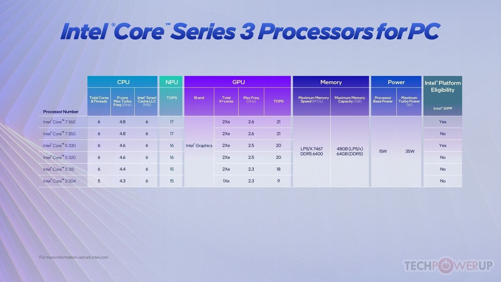
CHUWI today unveiled the UniBook, the world's first laptop powered by Intel's Wildcat Lake Core 3 304 processor (Core Series 3, Intel 18A, 5 cores/5 threads, up to 4.30 GHz). Primarily targeted for university students, entrepreneurs, and young professionals, the battery life can reach 15-20 hours (under comprehensive working conditions). Starting at an estimated $449, the UniBook directly challenges Apple's MacBook Neo with clear advantages in connectivity, keyboard backlight, display color accuracy, and price.

Key specs for CHUWI UniBook: 14-inch FHD (1920 x 1200) 100% sRGB IPS display, 8 GB LPDDR5X, 256 GB PCIe 3.0 SSD, Wi-Fi 6 + BT5.2, a full port suite (2x full-function USB-C, 1x HDMI 2.0, 2x USB 3.2 Gen 1, 1x USB 2.0, Gigabit Ethernet, TF card slot, 3.5 mm audio), white backlit keyboard, 180-degree hinge, active cooling, 53.38 Wh battery, and Windows 11 Pro.
The specifications follow.

Laptops Powered by Intel "Wildcat Lake" Arrive in China, Starting at $449

China appears to be the first in line to receive laptops powered by Intel's "Wildcat Lake" Core 300 series processors, and the initial models have already arrived. The most affordable option is the CHUWI UniBook, which features a five-core Intel Core 3 304 processor. This is the lowest in the series and the only five-core "Wildcat Lake" processor available. The laptop comes with 8 GB of LPDDR5X memory running at up to 7,467 MT/s and 256 GB of SSD storage. All of this is housed in a 14-inch body with a 1920x1200 IPS display. Interestingly, this model poses a direct challenge to Apple's MacBook Neo, operating on Windows 11 Pro and a different x86 platform.

Additionally, other laptop manufacturers have started listing their "Wildcat Lake" models on the Chinese retailer JD, including ASUS, HP, and Honor. These offerings include the ASUS Fearless 14SE 2026, HP OmniBook 3, and Honor Notebook X14 2026 Combat Edition. All three models are powered by the Intel Core 5 320 processor, which features a six-core design. They also come with 16 GB of LPDDR5X memory and 512 GB of SSD storage. The prices for these models are $597 for the ASUS, $571 for the Honor, and $662 for the HP OmniBook 3. These laptops offer twice the storage and memory compared to the popular Apple MacBook Neo, aiming to surpass Apple in the entry-level PC market. Interestingly, sales tax is not included in these prices.

Thermal Grizzly Releases New De-Lidded Intel Core Ultra 7 270K Plus CPUs

The Intel Core Ultra 7 270K Plus belongs to the Arrow Lake Refresh for Intel socket LGA1851 and delivers solid performance. With overclocking, the 270K Plus even surpasses the Intel Core Ultra 9 285K, the former Arrow Lake flagship. And it does so with a significantly better price-performance ratio. The best everyday temperatures for both processors are achieved with a direct-die water block in combination with liquid metal as the thermal interface material (TIM) and a custom water-cooling loop with as much radiator surface area as possible.

Delidded processors with a warranty provided by TG
The TG Delidded CPU is a processor that has been delidded by our trained staff and subsequently validated. During delidding, or "removing the lid," the processor's heatspreader is removed. While delidding and the use of corresponding direct-die coolers can significantly reduce temperatures under load, delidding results in the loss of the manufacturer's warranty. In the case of the TG Delidded CPU, Thermal Grizzly offers a warranty in addition to the legally required seller warranty.

ASUS Republic of Gamers Announces ROG NUC 16

ASUS Republic of Gamers (ROG) today announced the ROG NUC 16, a compact gaming PC powered by up to an Intel Core Ultra "Arrow Lake-HX" processor and an NVIDIA GeForce RTX 5080 Laptop GPU. Featuring an upgraded thermal design and patented removable stand for vertical or horizontal placement, the ROG NUC 16 is built for gaming, creative pursuits, and AI workloads. Armed with the latest Intel Core Ultra 9 processor 290HX Plus, the ROG NUC 16 delivers improved gaming performance versus the previous-generation ROG NUC. It supports up to 128 GB of DDR5-6400 memory, ensuring smoother high-FPS gameplay and faster responsiveness.

Compact yet powerful, the ROG NUC 16 raises the bar with AI-enhanced performance. It features up to an NVIDIA GeForce RTX 5080 Laptop GPU and supports NVIDIA DLSS 4.5 with ML-based Super Resolution and Multi-frame generation for faster, smoother gameplay. Its updated Super Resolution transformer model delivers improved lighting, finer details, and clearer motion, benefiting real-time rendering, video editing, and up to 8K creative workloads. In addition, users can unleash creativity and generate images at unprecedented speed with NVIDIA Studio. For AAA gaming, DLSS 4.5 can reduce latency and generate up to five additional frames per rendered frame, enabling a more fluid and immersive experience. Combined with the Intel Core Ultra 9 290HX Plus processor, ROG NUC 16 delivers up to 2.3% better 3DMark performance than its predecessor.

Intel "Razor Lake-AX" to Feature up to 32 Xe3 GPU Cores

Intel's upcoming "Razor Lake-AX" processor is shaping up to be a top-tier gaming chip. Reports suggest that Intel is working on multiple SKUs, with the flagship configuration featuring up to 32 Xe3 cores in its integrated graphics chip. According to the latest leaks from long-time Intel leaker Jaykihn, the "Razor Lake-AX" iGPU will be available in two versions: a 16-core iGPU and a 32-core iGPU, both based on Intel's Xe3 graphics IP currently found in "Panther Lake." This would make "Razor Lake-AX" nearly three times as powerful as the current Arc B390, which powers Intel's PTL lineup. This suggests that "Razor Lake-AX" will be a large package with next-generation CPU core IP and a robust iGPU cluster. Reportedly, this GPU die will measure around 162.84 mm², which is a significant size for integrated graphics.

Earlier this week, we learned that Intel also plans to return to on-package memory with the upcoming "AX" chip. Although the company initially claimed that the Core Ultra 200V "Lunar Lake" was the last design with on-package memory, Intel is reportedly bringing back on-package LPDDR5X/LPDDR6 memory to "Razor Lake-AX." Additionally, it's unclear where Intel will manufacture this massive chip, but the large iGPU suggests a design powered by EMIB and Foveros 3D to interconnect various elements. Finally, the chip is expected to feature a BGA-4326 package with 4,326 pins, similar to what Intel's Xeon CPUs typically use. Do note that the image below is not a real Intel slide.

Razer Unveils the New Razer Blade 18: Desktop-class Performance for Gaming and AI

Razer, the leading global lifestyle brand for gamers, today announced the 2026 evolution of the Razer Blade 18, its most powerful Blade ever. Designed for gamers and AI developers, the Blade 18 extends beyond traditional gaming laptops into a true desktop-class platform, built to run advanced workloads locally, from high-speed AI inference to real-time rendering and feature development, within a single, unified system.

The Edge of Performance. Gaming Meets AI Development.
  • Built to sustain high performance while running local LLM inference, compiling large codebases, rendering video and 3D assets, and playing modern AAA games.
  • Intel Core Ultra 9 290HX Plus processor (24 cores, up to 5.5 GHz boost) with an integrated NPU delivering up to 13 TOPS of AI acceleration
  • Up to NVIDIA GeForce RTX 5090 Laptop GPU with 175 W TGP, 24 GB of VRAM, and next-generation RTX AI technologies
  • Brighter 18-inch dual-mode display for UHD+ 240 Hz and FHD+ 440 Hz experiences
  • Advanced vapor chamber cooling with a refined multi-fan design for sustained workloads
  • Desktop-class connectivity including Thunderbolt 5, Wi-Fi 7, 2.5 Gb Ethernet, a 5MP camera, and a six-speaker system powered by THX Spatial Audio+

Intel Arc GPU Graphics Drivers 101.8801 Beta Released

Intel today released the latest version of Arc GPU Graphics Drivers. Version 101.8801 Beta comes with optimization for "Forza Horizon 6," "LEGO Batman: Legacy of the Dark Knight," and "Subnautica 2." The drivers also fix a bug that causes "Battlefield 6" to exhibit intermittent corruption in certain maps during gameplay has been fixed for Arc-branded integrated graphics of Core Ultra 200V "Lunar Lake" processors and Core Ultra Series 1 "Meteor Lake" processors. Grab the drivers from the link below.

DOWNLOAD: Intel Arc GPU Graphics Drivers 101.8801 Beta

AMD EPYC CPUs Reach Record Server Revenue Share of 46.2%

AMD's server CPUs are experiencing significant success, as the company captured nearly half of the server CPU spending in Q1 2026. According to the latest data from Mercury Research, AMD's EPYC CPUs account for 46.2% of total server CPU spending—a new all-time high for AMD's server CPU portfolio, which has become a major success in data centers. Interestingly, this is achieved with only a 27.4% unit share, indicating that while AMD's CPUs may not constitute exactly half of the units sold, they command much higher average selling prices (ASPs) than the competition. This competition is primarily from Intel, the largest CPU vendor. Intel currently holds the majority of units sold at 54.9%, a decrease of 3.4% compared to Q4 2025. We lack data on revenue share for Intel CPUs, but given their majority in unit shipments and AMD's near half share in spending, it can be concluded that the ASP of Intel Xeon server CPUs is lower than that of AMD EPYC.

In the data center, Arm-based designs account for about 17.7% of unit shipments in Q1 2026, meaning nearly one in five CPUs was Arm-based. Whether these were third-party integrations from Ampere or other Arm CPU makers, or in-house CPU designs from companies like Google, AWS, or Microsoft, remains unclear. However, Mercury Research collects extensive data, lending confidence to these figures.

Lenovo Completes 2026 ThinkPad Portfolio with Expanded AI PCs

Lenovo today announced the latest additions to its 2026 ThinkPad portfolio, completing the rollout of its next-generation business devices with new ThinkPad X13 Gen 7 and ThinkPad L Series models. Designed to meet the evolving needs of enterprise customers, the expanded portfolio brings AI-enabled performance, enhanced mobility, and flexible deployment options to organizations of all sizes.

Building on its 2026 portfolio momentum, Lenovo continues to advance its vision of Smarter AI for All through a portfolio of devices designed to support more intelligent and efficient ways of working. Across the latest ThinkPad systems, users benefit from advanced performance alongside the reliability, security, and manageability required in enterprise environments.

Intel CPUs Set to Power Googlebook Laptops, with "Wildcat Lake" in Play

Google launched its "Googlebook" laptops yesterday, introducing a new intelligent platform that leverages Gemini AI, succeeding its Chromebook offerings. Initially, it was unclear what hardware Google would use for its upcoming laptop models. However, Intel announced that it has been collaborating with Google on these models, with Intel Core processors at the core of the platform. Google is likely to pair these laptops with Intel's latest Core Series 300 "Wildcat Lake" processors, which the company recently launched. This means that Googlebooks will feature an x86 platform based on Intel processors, with six CPU cores consisting of two "Cougar Cove" P-cores and four LPE "Darkmont" cores. They will also include an NPU 5 with 40 TOPS of INT8 data, an Xe display and media engine, and a GPU with up to two Xe3 cores, all built on Intel's 18A internal node.

However, Intel will not be the exclusive platform provider for Googlebooks. In an exclusive interview with Google VP John Maletis, ChromeUnboxed learned that Google has set strict requirements for its OEM partners, including specifications for CPU, memory, keyboard layout, and storage configurations for its upcoming devices. Since launch partners will also include Qualcomm and MediaTek, we can expect to see Arm-powered Googlebooks as well. Acer, ASUS, Dell, HP, and Lenovo will be participating in the launch of the new Googlebook lineup, with devices reportedly arriving this fall.

Intel "Razor Lake-AX" Could Bring Back On-Package Memory

Intel plans to reintroduce on-package memory in the future, with the "Razor Lake-AX" potentially being the product to carry this feature. This could be a successor to the "Nova Lake" generation, expected to arrive in late 2026. The last time Intel used on-package memory was with the "Lunar Lake" Core Ultra 200V series of CPUs, which included LPDDR5X-8533 memory in a single package alongside the CPU, GPU, and I/O die. Intel had previously stated that future CPU generations after "Lunar Lake" would use off-die memory, as sourcing and integrating additional memory modules in its SoCs is challenging, despite having technologies like EMIB and Foveros 3D to support integration. However, this decision seems to be reconsidered, as Intel is reportedly planning to integrate memory back on-package with "Razor Lake-AX."

Intel's AX variants of SoCs have long been rumored to offer significant integrated graphics capabilities to handle demanding graphics workloads. This lineup is intended to compete directly with AMD's "Halo" series, which includes "Strix Halo," "Gorgon Halo," and other future revisions like "Medusa Halo." Intel aims to achieve excellent iGPU performance, bundled with substantial integrated memory such as LPDDR5X or the upcoming LPDDR6 memory. Eventually, Intel might reintroduce HBM memory, similar to what it did with "Kaby Lake G," but we are still awaiting more details from rumors and leaks. Amidst a significant memory shortage in the PC gaming world, Intel would likely face challenges in acquiring sufficient DRAM stock. However, by the time "Razor Lake-AX" arrives in the coming years, the situation could be quite different.

HPE Introduces 64 TB Memory Server for Critical and Complex Business Workloads

HPE (NYSE: HPE) today announced the availability of HPE Compute Scale-up Server 3250, a purpose-built server for in-memory databases, engineered to deliver scalability, resilience, performance, and security for critical business transactional and analytics workloads. Powered by Intel Xeon 6 processors, HPE Compute Scale-up Server 3250 delivers the highest memory available as the first scale-up server validated by the SAP BW Edition HANA benchmark with at least 48 terabytes (TB) of memory.

"HPE Compute Scale-up Server 3250 raises the bar for business-critical infrastructure," said Krista Satterthwaite, senior vice president and general manager, Compute at HPE. "Designed for complex business applications like enterprise resource planning and customer relationship management systems, this system helps customers in ways competitive offerings cannot - allowing them to run faster transactions, gain insights in real time, and support analytics without slowing down business. With simpler operations, always-on reliability, and chip-to-cloud security - we're redefining what scale looks like for workloads with zero-tolerance downtime."

Intel CEO Confirms Ongoing Product Collaboration with NVIDIA

Intel's CEO, Lip-Bu Tan, has confirmed that the collaboration with NVIDIA is ongoing, and we are about to see the results of the partnership announced late last year. Yesterday, Carnegie Mellon University awarded an Honorary Doctorate in Science and Technology to NVIDIA CEO Jensen Huang for his outstanding contributions to the fields of accelerated computing and AI. Intel's Lip-Bu Tan had the honor of placing the doctoral hood on him. In a post on X, the Intel CEO confirmed that Intel and NVIDIA are still working together to "develop exciting new products," indicating that the long-promised integration of NVIDIA GeForce RTX GPUs within Intel SoCs is still in progress. What began as an initial investment from NVIDIA into Intel and an announcement of product collaboration is evolving into a much deeper integration of both companies into a unified ecosystem.

First, we look forward to seeing Intel chips that integrate third-party GPU IP, this time from NVIDIA, with its GeForce RTX graphics embedded in an Intel-branded package. Similar to the now almost forgotten "Kaby Lake G" collaboration with AMD, Intel plans to integrate third-party graphics into its x86 SoC, codenamed "Serpent Lake," which is scheduled to be the first joint collaboration between NVIDIA and Intel in a single chip package. Second, we anticipate customized x86 Xeon server processors for NVIDIA, which Intel has been producing for large hyperscalers like Amazon for years. NVIDIA is also integrating Intel Xeon processors alongside its custom "Grace" and "Vera" CPUs, with designs customized by Intel for their HGX AI server nodes.

SK hynix Eyes Intel EMIB 2.5D Packaging for HBM Memory

SK hynix is collaborating with Intel to utilize its Embedded Multi-die Interconnect Bridge (EMIB) 2.5D packaging technology for HBM memory. As SK hynix aims to diversify its supply chain and customers are increasingly considering Intel Foundry, the South Korean memory giant is exploring research and development efforts with Intel on 2.5D packaging technology. Intel's premier 2.5D packaging technology is its EMIB, which interconnects multiple silicon dies using bridges embedded in a packaging substrate. SK hynix is interested in integrating this technology into its HBM memory, presumably to bring its HBM4 memory modules up to standard for EMIB integration, should its AI chip partners choose Intel Foundry for advanced packaging of their next-generation solutions.

We have already covered that small silicon EMIB bridges—available in variants like EMIB-M with embedded MIM capacitors and EMIB-T with TSVs—provide low-cost, high-density shoreline connections ideal for logic-to-logic and logic-to-HBM interfaces. However, until now, SK hynix has been using TSMC and its CoWoS 2.5D packaging technology. As CoWoS is gradually reaching its limits and customers are seeking alternative packaging methods, EMIB is emerging as a strong candidate to continue the scaling of chiplets in many directions beyond the traditional reticle limit of 830 mm² of silicon area.

Apple Strikes Deal with Intel Foundry Services for Chip Production in the U.S.

Apple and Intel Foundry Services have reached a preliminary agreement to onboard Apple as a foundry customer for manufacturing of Apple Silicon on its latest foundry nodes, according to a Wall Street Journal report. The move could see Apple end its near-total reliance on TSMC for production of its chips. Apple is looking to leverage the Intel 18A foundry node that offers comparable transistor densities and electric characteristics as TSMC's 2 nm-class nodes. Intel manufactures chips on the Intel 18A node in the state of Oregon, and is building new facilities in Ohio that will cater to future nodes. The company also has chip packaging facilities in states such as Arizona and Nevada. The move could improve Apple's contribution to the U.S. Government's efforts to onshore manufacturing of chips and other strategic commodities.

PC Motherboard Sales Face Sharp 25%+ Decline Amid Weak Demand

PC motherboard sales are on track for some of the biggest corrections in recent times as manufacturers struggle with weak demand, according to a DigiTimes report. What began as AI data center expansion quickly started affecting consumer PC DIY endeavors, as severe silicon shortages across the industry drove DRAM and CPU demand so high that prices have increased significantly for DDR4 and DDR5 memory kits, while regular CPUs have also seen a large price increase. In response, PC motherboard makers are caught in the middle of this shortage, seeing their motherboard unit sales revised down significantly. The report notes that all Taiwanese motherboard makers have significantly lowered their 2026 shipment targets, with some experiencing more than a 25% decrease in projected unit sales.

Interestingly, it's not only CPU and memory shortages driving this lowered demand; there are indications that consumers have slowed down their NVIDIA GPU upgrade cycles, which is impacting new motherboard sales. Particularly with the "Blackwell" GPU generation, consumers began purchasing PCIe 5.0 motherboards to achieve the greatest performance increase. However, as these GPUs became rarer and more expensive due to the global DRAM shortage, consumers have become reluctant to upgrade. ASUS is projected to sell about 10 million motherboards in 2026, while MSI and GIGABYTE are now projecting sales of less than 10 million units each. This represents about a 25% yearly decrease from 2025 sales. The worst position is estimated for ASRock, which is expected to see a 30% decrease according to the report.

PCIe 8.0 Targets 1 TB/s Bandwidth and May Need a New Connector

PCI-SIG has released a small update on its upcoming PCIe 8.0 standard, with the draft milestone reaching version 0.5. Perhaps the most intriguing aspect of this draft update is not the performance itself, but the exploration of a new connector technology to support this high-bandwidth protocol. Last year, we learned that PCI-SIG plans to implement a 256.0 GT/s raw bit rate and 1 TB/s of bidirectional bandwidth in the x16 lane configuration. We had assumed that the protocol would continue using the familiar connector technology seen in previous PCIe updates. However, it turns out that the current connector might be a limiting factor, prompting the search for a replacement for the traditional PCIe electrical connection.

The traditional PCIe connector is a copper-based link with up to 16 lanes connecting graphics cards to a slot. In a full x16 lane configuration, the PCIe generation supported by the motherboard provides the best performance, offering the maximum bandwidth the platform can deliver. However, with a 256 GT/s raw bit rate, the connector provides about 1 TB/s of bidirectional bandwidth, which is eight times faster than the current PCIe 5.0 platform used with modern GPUs and CPUs. This indicates that the current physical layer facilitating communication between a GPU and a motherboard is nearing saturation with the advent of PCIe 8.0, necessitating the consideration of an alternative connection method.

AMD to Expand EPYC Lineup With Specialized CPUs for AI, HPC, and Cloud

AMD's CPU offerings will soon expand into more categories, specializing in different tasks and use cases. During the latest Q1 earnings call, AMD CEO Dr. Lisa Su confirmed that customers are increasingly interested in specialized EPYC solutions and that future CPU generations will cater to different customer needs. This means that agentic AI will receive a dedicated EPYC CPU SKU, HPC workloads will have their own EPYC CPU SKU, AI training and inference will get a separate EPYC SKU, and cloud workloads will have a distinct SKU. This expansion of task-specialized CPU designs will go beyond the "Venice" CPU platform, which is expected to be released this year. At CES 2026, AMD confirmed that EPYC "Venice" will be a highly dense CPU package with up to 256 cores and 512 threads of "Zen 6c" cores, while the regular "Zen 6" configuration will have a maximum of 96 cores and 192 threads.

With this generation of EPYC CPUs based on the "Zen 6" core IP, AMD will promote "Venice" CPUs broadly, while the "Venice" CPU generation will be complemented by the "Verano" CPUs. These appear to use the same "Zen 6" microarchitecture but have optimizations specifically designed for AI infrastructure. Contrary to previous assumptions that "Verano" would be a "Zen 7" IP, it is now confirmed to be part of the 6th-generation EPYC CPU family. This indicates that AMD is starting its CPU customization for different workloads as early as this year. As the server CPU market is projected to reach $120 billion by the end of this decade, less than 3.5 years away in 2030, it makes sense to have different CPU SKUs for each task and capture a significant portion of that revenue. Server CPUs are also expected to grow at a 35% compound annual growth rate, which is impressive for a relatively mature market.

Terafab's Cost Could Reach $119 Billion as First Phase Starts at $55 Billion

Elon Musk recently announced an ambitious project called Terafab, which he plans to build on Tesla's campus in eastern Travis County, Austin, Texas. Thanks to recent court hearings in Grimes County, Texas, we have learned that the first phase of the Terafab project is expected to cost $55 billion. However, if additional phases are constructed, this figure could rise to $119 billion. While this is an astonishingly high amount, it seems justified given Terafab's ambitious goals. Semiconductor manufacturing is one of the greatest marvels of the modern world, with only a few companies competing for the top spot. The engineering and scientific expertise required for building modern semiconductor manufacturing facilities is so rare that it is concentrated in just a few places around the globe.

The goal of Terafab is to consolidate the entire chip manufacturing process under one roof. The plant is expected to integrate several stages of semiconductor production at a single site, including logic fabrication, memory, packaging, testing, and mask production. This setup is unusual, as these steps are typically spread across multiple specialized facilities and companies. The idea behind Terafab is that consolidating these processes could accelerate development by allowing engineers to design, test, and revise chips with fewer delays, essentially enabling rapid prototyping. This contrasts with the traditional, lengthy process of manufacturing chips at one site, packaging them at another, and testing them in-house. A typical semiconductor fab for nodes below 3 nm costs over $20 billion, but that only covers silicon manufacturing. Terafab's goal to handle everything will push that cost astronomically high.

MemTest86 Adds Preliminary LPCAMM2 Testing Support

PassMark's MemTest86 update version 11.7 (Build 1000) has added preliminary testing for the LPCAMM2 memory type, primarily for Intel's "Meteor Lake" and "Arrow Lake" chips. This means that the latest memory form factor can now be tested using a standardized testing methodology. With the rise of LPCAMM2 appearances, it is only logical that MemTest86 adds support for this form factor, which we have started seeing on Lenovo ThinkBook 14+ and 16+ and Framework Laptop 13 Pro models, especially from major DRAM manufacturers such as CXMT and Samsung. CXMT's LPCAMM2 memory uses LPDDR5X-8533 modules, while Samsung's modules are running LPDDR5X-9600 memory stacks. Interestingly, with further support from SK hynix, Samsung, Micron, and now CXMT, LPCAMM2 is aiming to become a universal standard for memory. Since the upcoming DDR6 memory is scheduled to be the main driver behind (LP)CAMM2, having a memory testing tool is essential.
Below is the list of fixes and enhancements.

Apple Eyes Intel and Samsung Foundries for Chip Production in the U.S.

Companies like Apple are always seeking top-tier manufacturing for their Apple Silicon products, which range from the A-Series chips in iPhones and low-power MacBooks to the more powerful M-Series SoCs that power iPads and higher-end Macs. Manufacturing these custom processors has traditionally been handled by TSMC, but Bloomberg now reports that Apple has been in talks with both Intel Foundry and Samsung Foundry to manufacture some of its chips in the coming months. It has been known for some time that Apple is exploring Intel's 18A-P process design kits (PDKs). Apple has used version 0.9.1 of the PDK designed for Intel's 18A-P node. With performance, density, power, and other metrics meeting expectations, Intel could become Apple's source for advanced node production by 2027.

Additionally, Apple is reportedly waiting for Intel to release the 18A-P PDK version 1.0, which is on track to launch in the first half of 2026 or may have already been released to partners. Once available, Apple plans to start with the lowest-end M-series chip, used in MacBook Air and iPad Pro devices, as previously mentioned. This node is particularly interesting due to its performance characteristics, as the 18A-P can deliver a 9% performance increase at the same power level or achieve 18% power savings at the same performance level compared to the standard 18A. This is exactly what Apple is looking for. Coupled with better thermal conductivity, these designs should offer improved heat dissipation and performance compared to what Apple currently achieves with TSMC's 3 nm process in the M5 SoC.

Lattice Semiconductor to Buy AMI for US$1.65 Billion

Last week, news broke that Lenovo had bought Phoenix Technologies' firmware (BIOS) technology business and now it looks like AMI—also known as American Megatrends Inc—is about to get a new owner, namely Lattice Semiconductor. That leaves Taiwanese Insyde Software as the only independent UEFI/BIOS developer in a market that at least on the desktop side has been largely ruled by AMI and is likely to continue to be so, even with AMI now being a subsidiary to Lattice Semiconductor.

Lattice is offering US$1.65 billion in cash and stock for AMI, which is a privately held company today. For those unfamiliar with Lattice, the company makes a range of FPGA solutions for a wide range of markets and is a competitor with AMD's Xilinx subsidiary and Altera, which is part owned by Intel. It's not entirely clear what the synergy is between Lattice and AMI, but a statement by Lattice CEO Ford Tamer suggests that the company thinks it might help its customers "deploy complex systems faster and with greater confidence" under Lattice's "everywhere companion chip strategy". Time will tell if this will lead to changes to AMI's current customers or not, since as the biggest UEFI/BIOS vendor out there—used by almost all mainstream motherboard makers and many other x86/x64 hardware makers—they have something of a unique position in the market.

Gigabyte Unveils Z890 PLUS Series Motherboards

Gigabyte Technology Co., Ltd., a global leader in high-performance computer hardware, is excited to announce the official launch of its Z890 PLUS series motherboards. Engineered to maximize the value and power of the new Intel Core Ultra 200S Plus series processors, this lineup, led by the high-value Z890 AORUS ELITE PLUS, delivers a significant leap in gaming performance without the premium price tag.

High-Value Performance for Every Gamer
The Z890 PLUS series is specifically designed for enthusiasts who prioritize performance-per-dollar. By focusing on models like the Z890 AORUS ELITE WIFI7 PLUS, Gigabyte provides a feature-rich platform that supports the latest high-performance processors. Internal testing against Intel 14th Gen CPUs reveals that these new processors offer up to 28% better gaming performance. In separate internal benchmarks, the series also demonstrates up to 35% better productivity performance compared to the previous generation. These distinct improvements make the PLUS series the ideal choice for both modern competitive gaming and intensive creative workloads.
Return to Keyword Browsing
Nov 17th, 2026 14:45 CST change timezone

New Forum Posts

Popular Reviews

TPU on YouTube

Controversial News Posts