
News Posts matching #Rubin

Return to Keyword Browsing

NVIDIA to Use SK hynix and Samsung HBM4 for "Vera Rubin" Without Micron

NVIDIA's upcoming "Vera Rubin" AI systems are scheduled for late summer shipping in the form of VR200 NVL72 rack-scale solutions that will power the next generation of AI models. However, not every memory maker of HBM4 qualified for a design win, as Micron has reportedly fallen out of the equation, with only Samsung and SK hynix left to supply the precious HBM4 memory. According to leaked institutional notes from SemiAnalysis, which tracks the supply chain in great detail, SK Hynix will represent about 70% of the HBM4 supply for VR200 NVL72 systems, with Samsung getting the remaining 30% of the supply. For a major memory maker like Micron, there is reportedly zero commitment for the supply of HBM4 memory.

Interestingly, this is not the end of Micron's share of memory in NVIDIA VR200 NVL72 systems. Instead of HBM4, the company will supply LPDDR5X memory for "Vera" CPUs, which can be equipped with up to 1.5 TB of LPDDR5X, making up for the lost share with the HBM4. It is possible that Micron didn't qualify for the significant system upgrade that NVIDIA performed for VR200 NVL72, which went from the initial system target of 13 TB/s in March 2025 to 20.5 TB/s in September. However, at CES 2026, NVIDIA confirmed that the VR200 NVL72 system is now operating at 22 TB/s of bandwidth, marking a nearly 70% increase in system bandwidth, all derived from aggressive memory specification scaling that the company demanded from the memory makers.
No NVIDIA GeForce RTX 50 "SUPER" GPUs This Year, RTX 60-Series Also Pushed Back

Artificial Intelligence may be eating the world of software now, but gamers are suffering. According to The Information, NVIDIA has reportedly entirely postponed the launch of its GeForce RTX 50 "SUPER" refresh, as the company's executives are prioritizing AI accelerators over the gaming sector, which consumes precious cutting edge GDDR7 memory. The GeForce RTX 50 "SUPER" refresh was originally scheduled for an announcement at CES 2026, with shipping in Q1 or Q2 of 2026. However, the GDDR7 memory used in the SUPER lineup was a high-capacity 3 GB version, which NVIDIA managers in December deemed too important for gamers, postponing the refresh entirely.

The "SUPER" series was planned with denser GDDR7 memory modules, offering 3 GB of capacity per chip, increasing the memory configuration of the standard GeForce RTX 5070, RTX 5070 Ti, and RTX 5080. Initially, the RTX 5070 SUPER was planned with an upgrade to offer 18 GB, while the RTX 5070 Ti SUPER and RTX 5080 SUPER would each provide 24 GB of GDDR7 memory. As NVIDIA's AI GPU portfolio also uses the high-density GDDR7 memory, like the RTX PRO 6000 "Blackwell" and "Rubin CPX" the company has decided to instead prioritize this high-margin business, leaving gamers with inflated prices of the regular GeForce RTX 50-series.

Samsung HBM4 Reportedly Verified for NVIDIA "Vera Rubin" AI Platform, Could be Demoed at GTC '26

Last week, intriguing early details of Samsung's (up to) 2 nm custom HBM logic die designs turned up via South Korean semiconductor industry insiders. As expected, talk of really futuristic computer memory tech also included comparisons to less distant prospects. According to official roadmaps, development of 4 nm node process-based HBM4 (sixth generation) modules wrapped up in 2025. Last Sunday, an SBS Biz news article claimed that Samsung Electronics had: "recently passed the final quality test for HBM4 from NVIDIA plus AMD, and will begin mass production next month." On the Team Green front, this fresh verification and consequent full-on manufacturing phase, could lead to initial batches getting showcased at the upcoming GTC 2026 AI conference (March 16-19). Industry moles propose that Samsung HBM4 modules will be "immediately used" in the performance demonstrations of next-gen "Rubin" AI accelerator products. NVIDIA's current-gen "Blackwell" AI GPU designs rely on HBM3E. Industry experts believe that Samsung trailed behind main rivals during the era of HBM3 and HBM3E, but newer observations predict the South Korean giant's (potential) return to prominence in the High Bandwidth Memory market sector.

A few weeks ago—at CES 2026—NVIDIA announced an upgrade of "Vera Rubin" memory bandwidth. It is not (officially) clear whether this jump from 20.5 TB/s (September 2025 spec) to 22 TB/s was enabled by the utilization of Samsung HBM4 modules. SBS Biz outlined one major advantage: "Samsung's HBM4 is said to have the industry's highest specifications (over the closest competition), operating at 11.7 Gb/s, which is faster than the 10 Gb/s (JEDEC standard) required by NVIDIA and AMD. It is said that Samsung demonstrated its technological perfection by passing verification without redesign, despite a customer's request for increased performance last year." Additionally, the publication's anonymous sources reckon that "full-scale supply" will commence by June time, due to HBM4 being closely tied to Team Green's "Vera Rubin" manufacturing schedule. Recently, Quanta Computer's Mike Yang anticipated first shipments of server hardware—heading to hyperscaler customers—starting around late summer.

NVIDIA Offers "Vera" CPU as a Standalone Competitor to Intel's Xeon and AMD's EPYC Processors

NVIDIA's integration of AI systems now extends beyond GPUs with generic Arm CPUs. The company is introducing its high-performance "Vera" CPUs as a standalone product, marking its first entry as a competitor to Intel Xeon and AMD EPYC server-grade CPUs. NVIDIA CEO Jensen Huang confirmed this new venture in an interview with Bloomberg, stating, "For the very first time, we're going to be offering Vera CPUs. Vera is such an incredible CPU. We're going to offer Vera CPUs as a standalone part of the infrastructure. You can now run your computing stack not only on NVIDIA GPUs but also on NVIDIA CPUs. Vera is completely revolutionary... Coreweave will have to act quickly if they want to be the first to implement Vera CPUs. We haven't announced any of our CPU design wins yet, but there will be many."

The "Vera" CPU is equipped with 88 custom Armv9.2 "Olympus" cores that utilize Spatial Multithreading technology, allowing it to handle 176 threads through physical resource partitioning. These custom cores support native FP8 processing, enabling some AI workloads to be executed directly on the CPU with 6x128-bit SVE2 implementation. The chip offers 1.2 TB/s of memory bandwidth and supports up to 1.5 TB of LPDDR5X memory, making it ideal for memory-intensive computing tasks. However, with the CPU now being offered as a standalone solution, it is unclear whether there will be any classic memory options like DDR5 RDIMMs, or if the CPU will rely solely on SOCAMM LPDDR5X. A second-generation Scalable Coherency Fabric provides 3.4 TB/s of bisection bandwidth, connecting the cores across a unified monolithic die and eliminating the latency issues common in chiplet architectures. Additionally, NVIDIA has integrated a second-generation NVLink Chip-to-Chip technology, delivering up to 1.8 TB/s of coherent bandwidth for external "Rubin" GPUs.

NVIDIA Upgrades "Vera Rubin" Memory Bandwidth Ahead of AMD Instinct MI400 Launch

As we anticipate the first shipments of NVIDIA's "Vera Rubin" in late summer, it has been reported that NVIDIA upgraded its superchip multiple times since March to better compete with AMD's upcoming Instinct MI400 series of accelerators. According to SemiAnalysis, NVIDIA's initial target for the "Vera Rubin" VR200 NVL72 system was 13 TB/s in March, which was upgraded to 20.5 TB/s by September. However, at CES 2026, NVIDIA confirmed that the VR200 NVL72 system is now operating at 22 TB/s of bandwidth. Compared to AMD's Instinct MI455X accelerator, which has 19.6 TB/s, NVIDIA initially had inferior system bandwidth. They addressed this by using faster DRAM and improving interconnects between CPUs, GPUs, and the entire system.

In November, AMD compared the MI400 lineup to NVIDIA's upcoming "Vera Rubin" series, claiming similar compute performance and memory bandwidth but 1.5 times higher memory capacity and scale-out bandwidth. AMD claims it will deliver up to 40 FP4 and 20 FP8 PFLOPs, roughly twice the compute performance of the current MI350. The GPUs also transition to HBM4 memory from HBM3e, increasing capacity from 288 GB to 432 GB and raising total bandwidth from 8 TB/s to 19.6 TB/s. Each GPU provides 300 GB/s of scale-out bandwidth and adds broader AI data format support along with expanded AI pipelines. Two models are planned: the Instinct MI455X for large-scale AI training and inference, and the MI430X for HPC and AI.

First Shipments of NVIDIA "Vera Rubin" AI Servers Expected Around Late Summer

Last week, Quanta Computer's Mike Yang let slip details about the eventual arrival of NVIDIA "Vera Rubin" AI server hardware. The executive vice president/general manager mentioned potential first shipments—heading in the direction of hyperscalers—occurring by August of this year. According to Taiwan's Commercial Times, this prediction was disclosed during an official celebratory company event (on January 15). Additionally, the Quanta boss does not expect a widespread deployment at that point in time, and (consequently) significant revenue generated by sales of new "Vera Rubin" equipment. According to the exec's statements, "most" customers are already running operations based on current-gen "Grace Blackwell" GB200 and GB300, but Yang believes that common architectural traits will make transitions—onto the next-gen platform—much easier than before.

Industry observers have highlighted possible issues of moving from the "Grace Blackwell" chiplet-based design to the advanced packaging of "Vera Rubin." During CES, NVIDIA announced that full production of server-grade "Vera" CPUs and "Rubin" GPUs had kicked off. This Q1 2026 initiation has happened well ahead of a previous "by H2 2026" mass manufacturing goal. Team Green's forthcoming "Vera Rubin" NVL72 SuperCluster is classed as a premier rack-scale system. A larger "NVL144" variant was previewed last year, but this CPX platform seems to be further out from release. According to a mid-October report, an involved manufacturing partner was weighing up a loose "2026 volume production" window.

GeForce RTX 60-series Linked to Mysterious "GR20x" GPU Dies, 2H'27 Launch Predicted

A sizeable gap—not occupied by NVIDIA's heavily rumored, and possibly tenuous GeForce RTX 50 SUPER-series—has been noticed at this week's CES trade show. During kick-off hours, the North American giant's GeForce social media quietly declared that "no new GPUs will be announced" within the four-day-long event. Graphics card industry observers have seemingly become tired of pursuing mid-generation product refreshments, and have set their sights further along Team Green's timeline. Yesterday, kopite7kimi fielded a number of queries regarding a futuristic GeForce RTX 6000 graphics lineup. Logically, these next-gen designs could leverage "Rubin" GPU architecture—already previewed as a well-known property in enterprise fields.

Speculation from last September—hinging on NVIDIA's official unveiling of their "Rubin CPX" GPU, that sports CUDA cores—lead to a theory that "GR10x" dies would form the basis of truly next-wave gaming graphics cards. In early 2026, kopite7kimi has proposed the utilization of a different set of GPU dies—identified as the "GR20x" group (or "GR200" family). Specifically, the PC hardware sleuth has pinpointed an alleged "GR212" model. They surmise that NVIDIA's "Rubin" architecture-based GeForce RTX 60-series will arrive within a second half of 2027 launch window.

NVIDIA DGX SuperPOD Sets the Stage for Rubin-Based Systems

NVIDIA DGX SuperPOD is paving the way for large-scale system deployments built on the NVIDIA Rubin platform—the next leap forward in AI computing. At the CES trade show in Las Vegas, NVIDIA today introduced the Rubin platform, comprising six new chips designed to deliver one incredible AI supercomputer, and engineered to accelerate agentic AI, mixture-of-experts (MoE) models and long-context reasoning. The Rubin platform unites six chips—the NVIDIA Vera CPU, Rubin GPU, NVLink 6 Switch, ConnectX-9 SuperNIC, BlueField-4 DPU and Spectrum-6 Ethernet Switch—through an advanced codesign approach that accelerates training and reduces the cost of inference token generation.

DGX SuperPOD remains the foundational design for deploying Rubin-based systems across enterprise and research environments. The NVIDIA DGX platform addresses the entire technology stack—from NVIDIA computing to networking to software—as a single, cohesive system, removing the burden of infrastructure integration and allowing teams to focus on AI innovation and business results. "Rubin arrives at exactly the right moment, as AI computing demand for both training and inference is going through the roof," said Jensen Huang, founder and CEO of NVIDIA.

NVIDIA Powers Nearly 72% of Cloud Accelerator Locations, AMD at 5.8%

The cloud accelerator market share study was conducted at UBS bank, one of the leading research hubs and close followers of market trends. According to UBS, NVIDIA commands 71.2% of the cloud accelerator location share, which includes GPUs and other types of ASICs. The study also included AMD, and other ASICs. For the AMD front, the situation is entirely different as the data shows AMD only captures 5.8% of the cloud accelerator location share. The remaining portion is split between ASICs designed by the likes of AWS, Meta, Broadcom, MediaTek, and many others, which command 22.3%.

For NVIDIA, the company has managed to penetrate its GPUs in 258 datacenter locations, serving as cloud GPU providers. This is a significant number considering that some of these customers are ordering tens and even hundreds of thousands of GPUs at once, especially as the demand expands. NVIDIA is still the backbone of the entire AI infrastructure, and even its older GPUs, which include A100 and H100, are capturing a significant part of the GPU cloud market share. As "Blackwell" SKUs, designed for a million GPU scale systems, are scaled, and we enter the "Rubin" era, NVIDIA's lead may only expand.

SK Hynix Slows Down HBM4 Ramp, Prepares 300+ Layer NAND Flash

Interesting developments are unfolding in the world of DRAM and NAND flash, as one of the largest players, SK Hynix, has announced product updates for 2026. The company appears to be following its competitor Samsung by slowing the ramp-up of its next-generation HBM4. Initially, SK Hynix planned to increase its HBM4 capacity in the second quarter of 2026. However, this has been postponed to the third quarter of 2026, as the company plans to expand its HBM4 manufacturing capacity. The delay is due to the high demand for its current HBM3E capacity, necessitating the continued operation of HBM3E manufacturing sites longer than expected. SK Hynix's largest customer for HBM chips, NVIDIA, is reportedly facing challenges with the volume production of "Rubin," delaying the need for HBM4, while the HBM3E-equipped "Blackwell" remains in strong demand.

Samsung Secures Deal to Supply Half of NVIDIA's SOCAMM2 Modules in 2026

Korean tech publication Hankyng reports that Samsung Electronics has secured a deal to supply half of NVIDIA's SOCAMM2 modules in 2026. NVIDIA designed its upcoming "Vera Rubin" Superchip module, which consists of two "Rubin" AI GPUs and one "Vera" CPU, to support DDR5 SOCAMM2 modules. These replace hardwired LPDDR5X ECC memory found in current "Grace Blackwell" Superchip modules. SOCAMM2, or small-outline CAMM2, is a variant of DDR5 CAMM2 modules with slimmer outlines, to further minimize their PCB footprint. Replacing 512-bit LPDDR5X on Grace with 8-channel (16 sub-channel) DDR5 on Vera allows for higher densities that are further upgradeable, and higher clock speeds.

Samsung HBM4 Development Complete, Mass Production Pending NVIDIA Approval

Samsung has reportedly finished development of its first sixth-generation HBM (HBM4) chips and is now in the final pre-mass-production stage. According to new reporting from AjuNews and Korean industry sources, Samsung's Device Solutions division has cleared Production Readiness Approval (PRA), the last internal checkpoint before full-volume manufacturing. HBM4 is expected to deliver roughly 60% higher bandwidth than the current HBM3E chips. Samsung has already shipped HBM4 samples to NVIDIA, which is evaluating them for use in its upcoming Rubin platform. Initial samples have already exceeded NVIDIA's next-gen GPU requirement of 11 Gbps per pin. The company is using improved 1c-class DRAM paired with a 4 nm logic base die, a combination that helps close the gap with rivals while keeping thermals and power in check at these higher speeds. Once NVIDIA signs off, Samsung can move straight into volume production, with manufacturing lines already prepared.

Samsung had already signaled strong progress during its Q3 2025 earnings call on October 30, noting that HBM4 samples were in the hands of global customers and that mass production is planned for 2026. "HBM3E is currently in mass production and being sold to all related customers, while HBM4 samples are simultaneously being shipped to key clients," the company said at the time. Samsung also confirmed that its foundry arm will prioritize stable 2 nm GAA output and HBM4 base-die production in 2026, alongside the ramp of its new Taylor, Texas fab. The company is also said to be working on a faster HBM4 variant targeting another 40% performance uplift, with an announcement possible as early as mid-February 2026.

NVIDIA Reportedly the Only TSMC A16 Node Customer

NVIDIA is reportedly the only customer queued for TSMC's next-generation A16 process, and the company is lining the node up for its upcoming "Feynman" GPUs. The company is lining up for samples in 2026 with volume ramps following in 2027, timing that would slot "Feynman" after "Rubin"-class products built on refined 3 nm variants. If the reports are accurate, NVIDIA's commitment would be notable as it would be the only major company opting for the "stopgap" node between N2 and A14. Customers like Apple are reserving TSMC N2 2 nm capacity and plan to transition to A14 as soon as it becomes available, bypassing the A16 node.

TSMC's A16 node is a nanosheet-focused design featuring enhanced backside power delivery, known as Super Power Rail (SPR). This design separates power routing from signal layers, reducing delivery losses. The process is expected to provide modest single-digit performance improvements, more noticeable power reductions for AI workloads, and slightly higher transistor density compared to the previous generation. For very large dies and high-power cards, these enhancements can lead to cleaner floorplanning, easier thermal management, and increased capacity for memory and interconnect bandwidth. While these improvements are significant for NVIDIA's datacenter chips, Apple's mobile and laptop chips may benefit even more from the less expensive N2 node and its variations.

Intel Sees 5,000 W GPUs Possible with Integrated Voltage Regulators

If the performance requirements for new AI or HPC tasks demand maximum performance density regardless of power or heat constraints, Intel has a project presentation scheduled for the ISSCC conference in February 2026. One of the topics will be a 5,000 W GPU design utilizing integrated voltage regulators (IVRs). While this may seem extreme, Intel plans to leverage advanced packaging technology, specifically the Foveros-B variant, to deliver 5 kW GPUs by 2027. As accelerators scale to support larger AI and HPC workloads, traditional board-level regulators are hitting limits in current density and transient response.

Moving voltage regulation into the package shortens current paths and reduces delivery losses. Intel Foundry and its packaging division are already exploring high-density power delivery and kW-class integrated voltage regulators. Intel's Foveros roadmap targets production-ready integrated power elements by 2027, enabling customers to evaluate IVR-enabled assemblies at scale very soon. While Foveros-B is a 2027 product, customers could potentially evaluate multi-kilowatt designs with IVRs next year. Intel is not a singled-out player with multi-kilowatt designs, as NVIDIA "Rubin" silicon is rumored to have a TDP of up to 2.3 kW for highest-end models, leading to rack-level power consumption exceeding 250 kW.

NVIDIA May Stop Bundling Memory with GPU Kits Amid GDDR Shortage

NVIDIA is rumored to be changing its approach by supplying only the raw silicon to its AIC partners, rather than bundling its usual GPU and memory kit. Typically, GPU manufacturers like NVIDIA, AMD, and Intel provide their GPU dies with GDDR memory to AIC partners as a kit. These partners then solder the components onto their custom PCBs, often modifying the layout and cooling systems. However, according to Golden Pig Upgrade, NVIDIA might halt this practice and supply only the bare silicon dies due to memory shortages affecting the company's ability to meet orders.

Recently, AMD informed its supply chain of an impending price increase across its entire GPU product line by about 10%. This decision is primarily driven by a significant memory shortage, which has led to soaring DRAM prices and reduced profit margins for GPU manufacturers. AMD's AIB partners have been advised of the planned 10% price hike, and it is expected that AIBs will follow suit in the coming weeks to maintain their margins. However, this now adds to the entire confusion of DRAM shortage, especially for GPUs.

Next-Gen HBM Targets Embedded GPU Cores

Tech companies are exploring a major shift in HBM design seeking to embed GPU cores directly into next-generation memory stacks. According to Korean industry reports, Meta and NVIDIA are evaluating "custom HBM" architectures that integrate GPU cores into the base die of future HBM devices, with SK Hynix and Samsung said to be involved in early discussions. HBM stacks multiple DRAM dies on top of a base die that handles external I/O. HBM4 is expected to reach mass production next year and will include an onboard controller to improve bandwidth and efficiency. Integrating GPU cores would take this concept several steps further, distributing compute into the memory itself to reduce data movement and cut power usage. Industry sources say the approach could boost both performance and energy efficiency for AI workloads by cutting the distance between compute and memory. But the design still faces major struggles such as limited die area in Through-Silicon Vias (TSV) based stacks, power delivery constraints, and the difficulty of cooling those compute-heavy GPU logic inside the base die.

Kim Joung-ho, a professor in the School of Electrical Engineering at KAIST, said, "The speed of technological transition where the boundary between memory and system semiconductors collapses for AI advancement will accelerate," and added, "Domestic companies must expand their ecosystem beyond memory into the logic sector to preempt the next-generation HBM market." AMD's recently unveiled Instinct MI430X accelerator built on the next-generation AMD CDNA architecture supports 432 GB of HBM4 memory and 19.6 TB/s of memory bandwidth. NVIDIA's "Vera Rubin" Superchip takes a different approach. Each Rubin GPU integrates two reticle-sized compute chiplets paired with eight HBM4 stacks, delivering around 288 GB of HBM4 per GPU and roughly 576 GB of HBM4 across the full Superchip. From those potential changes companies that have strong packaging and logic capabilities will benefit, while pure memory vendors may need to expand into system-level semiconductor technologies to stay competitive.

NVIDIA Moves to In-House Server Production, Leaving OEMs with a Secondary Role

NVIDIA plans to reshape the industry's approach to building high-performance AI servers with its "Vera Rubin" product stack, which will enter volume production as the VR200 line in late 2026. Rather than supplying CPUs and GPUs to OEMs, NVIDIA plans to ship fully finished L10 compute trays that come pre-populated with "Vera" CPUs, "Rubin" accelerators, memory, 800G NICs, 110kW power delivery, and liquid-cooling infrastructure, all of which are validated before they leave the factory. This, however, will leave many system vendors and OEMs shifting away from designing core server electronics and toward tasks such as rack-level assembly, power configuration, installation of rack cooling sidecars, and final certification.

Rubin silicon is rumored to have a TDP of up to 2.3 kW for highest-end models, leading to rack-level power consumption exceeding 250 kW and making custom cooling designs economically unviable. NVIDIA's strategy reportedly involves standardizing cooling and power across two performance tiers while increasing network I/O density. These choices decrease the feasibility and cost-effectiveness of third-party replication. By centralizing production with select partners, development cycles can be shortened and manufacturing yields improved. However, this approach also limits the options OEMs and hyperscalers have traditionally used to differentiate their hardware.

HPE Unveils Newest Additions to Its Next-Generation Cray Supercomputing Portfolio

HPE (NYSE:HPE) today announces the newest additions to the next-generation HPE Cray supercomputing portfolio that provide industry-leading compute density, designed to meet the needs of artificial intelligence (AI) demands while performing at-scale. This HPE Cray Supercomputing portfolio expansion includes three multipartner, multi-workload compute blades, unified management software and high-performance interconnect support, establishing one of the most powerful supercomputing architectures in the industry for research laboratories, sovereign entities and large enterprises that are increasingly turning to AI to advance their simulations and drive scientific discovery.

"Global organizations relying on supercomputing are looking for better computing performance for all of their workloads," said Trish Damkroger, senior vice president and general manager, HPC and AI Infrastructure Solutions at HPE. "Our new HPE Cray Supercomputing platform is the answer to customers' needs for higher performance density with a unified AI and HPC architecture that is engineered for groundbreaking outcomes. HPE is proud to share our unwavering commitment to AI and supercomputing as the engine of innovation and scientific discovery, advancing the way people live and work."

NVIDIA First Company in History at $5 Trillion Value After Major Announcements at GTC 2025

NVIDIA's stock jumped 5% on Tuesday, closing at a record high and pushing the company's valuation to $4.89 trillion, just shy of the $5 trillion milestone. The surge followed a wave of new announcements at its GTC event in Washington, D.C., covering AI, supercomputing, and major industry partnerships. NVIDIA's shares have risen more than 50% year-to-date, more than doubling since April, fueled by demand for GPUs powering cloud data centers from Amazon, Google, and Microsoft. The company has also invested up to $100 billion in OpenAI, one of its largest customers. In his keynote, CEO Jensen Huang said that it is expecting $500 billion in GPU sales by the end of 2026, a realistic target if we consider that NVIDIA generated over $100 billion in revenue in just the first two quarters of this year.

During the GTC event NVIDIA revealed plans with the U.S. Department of Energy to build seven new supercomputers including one powered by 10,000 Blackwell GPUs. NVIDIA also introduced NVQLink, a new open systems architecture designed to accelerate the development of quantum supercomputers. Moreover, NVIDIA yesterday showcased its highly anticipated "Vera Rubin" Superchip, a single package combining two Rubin GPUs with a Vera CPU featuring 88 cores and 176 threads. While competition from AMD, Qualcomm, and in-house chips developed by hyperscalers continues to grow, NVIDIA remains positioned at the center of the AI infrastructure boom edging closer to the $5 trillion milestone valuation that seems set to become reality in a matter of days.

Update 18:31 UTC: NVIDIA's finance team has clarified that CEO Jensen Huang's reference to "$500 billion in GPU sales by the end of 2026" during his GTC keynote was misinterpreted. The figure refers to cumulative sales from the Blackwell and Rubin platforms over roughly two years—through calendar 2026 or fiscal 2027—not over the next five quarters. Analysts confirmed the correction following discussions with CFO Colette Kress's team. NVIDIA also reiterated its long-term goal of reaching $1 trillion in annual revenue later this decade. However, the revised guidance remains well above Wall Street expectations and does not yet consider the potential China-related sales, which could boost future figures.

Update 15:42 UTC: NVIDIA just crossed $5 trillion milestone, reaching $5.14 trillion valuation. A quick reminder, the company was valued at $10 billion ten years ago. It then hit the $1T milestone in May 2023, $2T in March 2024, $3T in June 2024, and $4T this July.

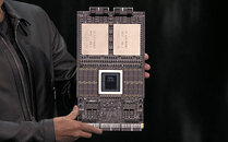
NVIDIA's "Vera Rubin" Superchip System Pictured for the First Time

NVIDIA yesterday had a GTC conference in Washington D.C., showing its latest "Vera Rubin" Superchip symbiote. Pictured for the first time is the combination of two "Rubin" GPU paired with a single "Vera" CPU carrying 88 custom NVIDIA cores and 176 threads in a single package. NVIDIA quoted performance targets of roughly 50 PetaFLOPS of FP4 compute per Rubin GPU, which yields about 100 PetaFLOPS FP4 for the two-GPU Superchip. The company said engineering samples are already moving through labs and set mass production goals for 2026 with broader shipments and deployments into 2027.

Each Rubin GPU appears to integrate two reticle-sized compute chiplets (2x830mm²?) paired with eight HBM4 stacks, delivering about 288 GB of HBM4 per GPU and roughly 576 GB of HBM4 on the full Superchip. NVIDIA also populated the board with SOCAMM2 LPDDR5X modules to provide large, low-latency system memory, with some older briefings indicating around 1.5 TB of LPDDR5X per Vera CPU on typical trays. The Vera CPU itself uses an 88-core, 176-thread Arm-based custom design and shows signs of a multi-chiplet layout with a distinct I/O chiplet nearby. With "Grace," NVIDIA relied on Arm's Neoverse design, but with Vera, the design team brought this CPU core in the house to extract maximum performance. Additionally, NVLink bandwidth climbs to approximately 1.8 TB/s to sustain heavy CPU-to-GPU traffic in system-demanding workloads such as AI inference and training.

HPE to Build "Mission" and "Vision" Supercomputers Featuring NVIDIA Vera Rubin

HPE today announced, in partnership with the U.S. Department of Energy (DOE), National Nuclear Security Administration (NNSA) and Los Alamos National Laboratory (LANL), that it has been selected to deliver two state-of-the-art supercomputers, named "Mission" and "Vision". The next-generation systems will be based on the new direct liquid-cooled HPE Cray Supercomputing GX5000 system and feature upcoming NVIDIA Vera Rubin Superchips. Mission and Vision are part of the DOE's $370 million investment to accelerate scientific discovery, advance AI initiatives and strengthen national security.

"For decades, HPE and Los Alamos National Laboratory have collaborated on innovative supercomputing designs that deliver powerful capabilities to solve complex scientific challenges and bolster national security efforts," said Trish Damkroger, senior vice president and general manager, HPC & AI Infrastructure Solutions at HPE. "We are proud to continue powering the lab's journey with the upcoming Mission and Vision systems. These innovations will be among the first to feature next-generation HPE Cray supercomputing architecture to drive AI innovation and scientific impact."

NVIDIA to Build Seven New AI Supercomputers for U.S. Government

NVIDIA today announced that it is working with the U.S. Department of Energy's national labs and the nation's leading companies to build America's AI infrastructure to support scientific discovery, economic growth and power the next industrial revolution.

"We are at the dawn of the AI industrial revolution that will define the future of every industry and nation," said Jensen Huang, founder and CEO of NVIDIA. "It is imperative that America lead the race to the future—this is our generation's Apollo moment. The next wave of inventions, discoveries and progress will be determined by our nation's ability to scale AI infrastructure. Together with our partners, we are building the most advanced AI infrastructure ever created, ensuring that America has the foundation for a prosperous future, and that the world's AI runs on American innovation, openness and collaboration, for the benefit of all."

NVIDIA Prepares New Driver Era for "Rubin" GPUs in 2026

NVIDIA appears to be gearing up for software support for "Rubin," the architecture expected to succeed "Blackwell," after a set of driver patches introduced a new identification register called BOOT_42. The initial patches landed on public mailing lists late on a Friday and include a change titled for next-generation GPUs. In the patch cover letter, NVIDIA engineer John Hubbard explains that architecture and revision metadata will transition from NV_PMC_BOOT_0 to NV_PMC_BOOT_42, with BOOT_0 being cleared. These updates were submitted to the Nova kernel driver tree, which is serving as the public platform for this early work. The patches adjust the detection path so the driver can recognize devices from Turing onward using the new register layout.

The submission also adds comments that document how BOOT_0 and BOOT_42 evolve across GPU generations, and it removes a couple of legacy types, Spec and Revision. According to the notes, this simplification removes some complexity and makes future boot42 support updates easier to follow, avoiding generation-specific adjustments when new revisions arrive. The changes confirm that current generations from Turing through Blackwell will continue to use BOOT_0 while future, post-Blackwell chips will be identified solely via BOOT_42. Targeting Rubin, this work is another example where NVIDIA is actively preparing driver support ahead of hardware launch. If Rubin enters volume production in the second half of 2026 as previously reported, having the identification and selection logic ready in advance should help reduce the gap between shipments and software enablement, meaning that fast-moving hardware release cycles will be followed very closely with optimized software.

NVIDIA "Vera Rubin" NVL144 Servers Set for 2026 Volume Production

Foxconn has begun engineering validation for NVIDIA's "Vera Rubin" NVL144 MGX liquid-cooled racks, with plans for mass production in the latter half of 2026, according to internal supply-chain documents obtained by Taiwan Economics Daily. Each NVL144 unit features 144 Rubin GPUs with HBM4, updated 88-core Vera CPUs, and ConnectX-9 NICs and NVLink 6 interconnect for CPU-to-GPU and GPU-to-GPU communication, effectively doubling the compute density of the current NVL72 platform. The Taiwanese contractor Foxconn currently handles about 60% of NVIDIA's AI server output and is expanding its immersion-cooling and copper-plating lines at its Wisconsin and Houston facilities to meet new domestic manufacturing requirements.

The gap between GB300 peak shipments and Rubin's first silicon will be six to eight months, the shortest generational gap in NVIDIA's history. Despite the accelerated roadmap, Blackwell Ultra remains NVIDIA's main revenue source through mid-2026. Procurement data shows that cloud providers have reserved around 400,000 GB300 nodes for delivery in late 2025 and early 2026, indicating strong near-term demand. At the same time, OpenAI has placed a large preorder for Vera Rubin silicon, securing initial production volumes and supporting Foxconn's capacity investments. The rapid transition from Hopper to Blackwell and then to Rubin within 30 months marks the fastest acceleration of datacenter equipment cycles, leading hyperscale operators to speed up depreciation schedules.

Frore Systems introduces LiquidJet, Coldplate for AI Data Centers

Frore Systems today announced the launch of LiquidJet, a revolutionary direct-to-chip liquid cooling 3D coldplate solution designed to meet the escalating demands of AI Data Centers. Built with Frore's unique semiconductor manufacturing process adapted to metal wafers, LiquidJet unlocks higher performance from the world's most powerful GPUs—starting with NVIDIA Blackwell Ultra—delivering significant reductions in data center total cost of ownership (TCO).

"LiquidJet's unique 3D architecture, with customized short-loop jet channel microstructures, sets a new bar for coldplate thermal performance," said Seshu Madhavapeddy, CEO and Founder of Frore Systems. "Just as AirJet redefined active cooling for consumer and edge devices, LiquidJet transforms coldplates into a future-ready platform for the AI Factory."
Return to Keyword Browsing
Nov 18th, 2026 13:38 CST change timezone

New Forum Posts

Popular Reviews

TPU on YouTube

Controversial News Posts