Monday, December 8th 2025

SK Hynix Slows Down HBM4 Ramp, Prepares 300+ Layer NAND Flash
Interesting developments are unfolding in the world of DRAM and NAND flash, as one of the largest players, SK Hynix, has announced product updates for 2026. The company appears to be following its competitor Samsung by slowing the ramp-up of its next-generation HBM4. Initially, SK Hynix planned to increase its HBM4 capacity in the second quarter of 2026. However, this has been postponed to the third quarter of 2026, as the company plans to expand its HBM4 manufacturing capacity. The delay is due to the high demand for its current HBM3E capacity, necessitating the continued operation of HBM3E manufacturing sites longer than expected. SK Hynix's largest customer for HBM chips, NVIDIA, is reportedly facing challenges with the volume production of "Rubin," delaying the need for HBM4, while the HBM3E-equipped "Blackwell" remains in strong demand. SK Hynix is moving forward with its 3D NAND roadmap by developing a new 300-layer, tenth-generation (V10) module that will use wafer-to-wafer hybrid bonding. The company plans to validate this technology on a V10 test line in 2026 and begin full-scale production in 2027. Unlike the current 321-layer V9, which uses a single-wafer peri-under-cell (PUC) approach, the new V10 NAND flash will produce the memory cell stack and peripheral circuitry on separate substrates and then bond them together. This separation reduces the thermal and process stress on peripheral circuits during the formation of tall stacks and can shorten cycle times since the two wafers are processed independently. However, this approach increases process complexity significantly. Wafer alignment and bonding must achieve nanometer-scale precision across hundreds of dies, requiring advanced hybrid-bonding equipment and stricter yield control.
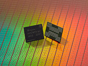 All of this may sound promising for the long term, but addressing the recent industry shortages of NAND and DRAM can't be satisfied with new production capacity scheduled for late 2026 and 2027. SK Hynix plans to continue capital investment to advance V10 while converting significant capacity to V9 production, shifting tens of thousands of 12-inch wafers per month into higher-layer output to meet rising enterprise SSD demand, which will help alleviate some of the demand in the future. However, the next few quarters may still face limited NAND flash capacity as existing output is converted to new technology. For DRAM, there doesn't seem to be a significant increase, but SK Hynix has recently begun installing more EUV machines, which could become operational in the coming quarters. SK Hynix reportedly plans to install 20 Low-NA EUV units in the next two years, all designed for HBM memory and advanced storage solutions.
Sources:
Hankyuang, ZDNet Korea, via harukaze on X


8 Comments on SK Hynix Slows Down HBM4 Ramp, Prepares 300+ Layer NAND Flash
What happened to the consumer 321 layer NAND products that supposedly entered production in August 2025?
"The company plans to apply its 321-layer NAND first to PC SSDs, before expanding to enterprise SSDs (eSSD) for data centers and UFS for smartphones."
I guess plans changed?
SK hynix Begins Mass Production of 321-Layer QLC NAND Flash August 24, 2025
fuck you Hynix you sad fucks, between you Crucial and Samsung, none of you are worth more than the other, you make good tech but you always forget to remember who was a large share of your revenue before tech investments exploded like it did some time ago, y'all sure were happy to have us buy your sticks and graphics cards, huh Nvidia?
www.yolegroup.com/industry-news/sk-hynix-announces-production-of-its-321-layer-nand-flash-shipments-will-start-in-the-first-half-of-2025/
So I think even if it comes to consumer sector early, we're gonna get some novelty small form up to 4 TB drive with extremely high price "because it's completely new tech" - although it won't be anything stellar due to being QLC.