News Posts matching #Tremont

Return to Keyword Browsing

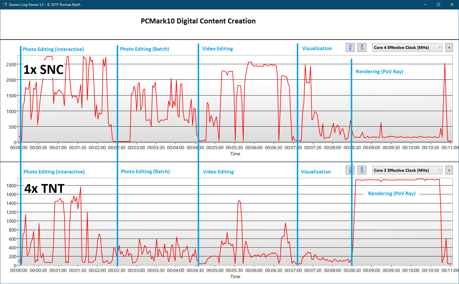
Akasa Intros Newton CAC Fanless Case for Intel Atlas Canyon NUC

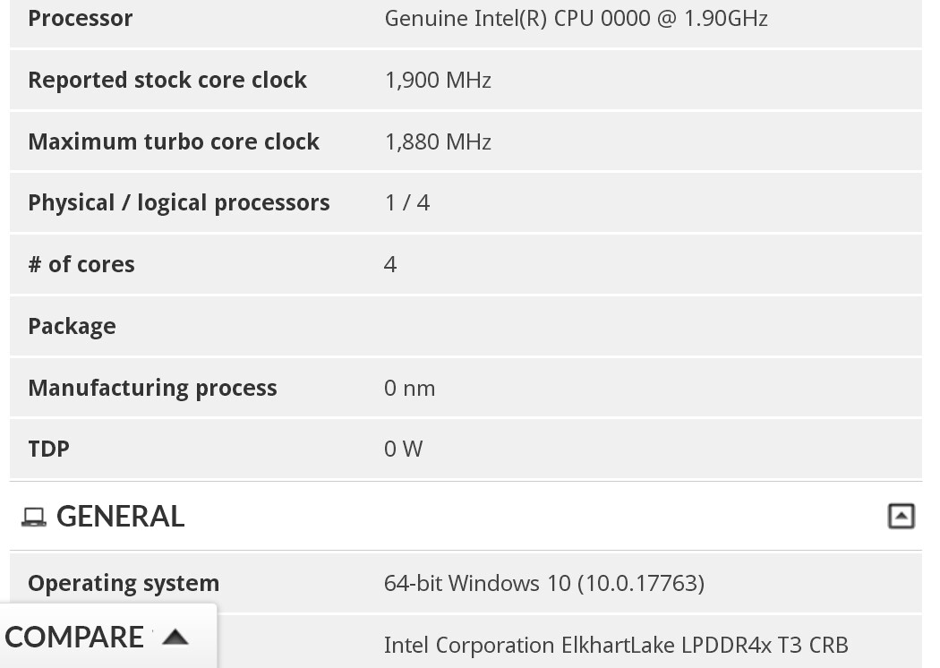
Akasa today introduced the Newton CAC fanless case for the entry-level Intel Atlas Canyon NUC boards. These NUCs are based around the Pentium Silver 6000-series and Celeron 4500-series "Jasper Lake" SoCs featuring up to 4 "Tremont" E-cores. The Akasa case offers full fanless cooling for the SoC, letting you use it as a digital-signage or AIoT box. The case has cutouts for nearly all of the Atlas Canyon's connectors, except the 9-pin external header for an additional front-panel. The case is made of anodized-aluminium with a ridged surface for heat-dissipation. The front- and rear-panels feature a brushed-aluminium finish with diamond-cut edges. It measures 178 mm x 117 mm x 44 mm. The company didn't reveal pricing.

Chuwi Announces MiniBook X Laptop with Hole-Punch Camera

MiniBook X comes loaded with the latest generation Intel 11th Celeron N5100 processor, including 10 nm process technology, quad-core and four threads, new Tremont microarchitecture, and a 10 W thermal power consumption design that ups the power while lowering the consumption. MiniBook X handles document editing, basic video production, and modern gaming with increased efficiency, while next-gen Intel UHD Graphics makes it easy to decode 4K video and fluidly handle online games.

As an enhanced and upgraded version of MiniBook, MiniBook X introduces a 10.8-inch hole-punch display with 2K retina resolution, 90% screen-to-body ratio and a 16:10 aspect ratio for a shockingly immersive viewing experience. Chuwi has also added YOGA Mode to MiniBook X, giving it the 2 in 1 functionality of both a laptop and tablet and the ability to switch back and forth as needed quickly.

MSI Announces Cubi N Mini PCs Powered by Intel "Jasper Lake"

MSI, a world leader in high-performance and innovative computing solutions, announced the Cubi N JSL Business & Productivity PC. Featuring small chassis, powerful processor, exclusive software, and various IO ports, the Cubi N is designed with efficiency and productivity in mind.

The Cubi N mini PC kit with 0.5L in size is ready to defy your imagination. The tiny design allows you to have a well-organized and efficient working space without limiting your capability of being productive and effective. Equipping Intel Jasper Lake Processor built on 10 nm "Tremont" delivers up to 30% IPC performance boost that improves your computing experience while working. It provides better performance for users while scalability, durability, VESA Mount support, and upgradable design that is time-saving and space-saving allow users to use it in any kind of situation. The low noise and power-saving features provide users a better quality of life and can even avoid bothering others in the same space including office, home, or dormitory.

Intel NUC 11 Essential Detailed: Powered by Pentium Silver and Celeron "Jasper Lake"

Intel is giving finishing touches to the NUC 11 Essential, its next-generation entry-level NUC desktops powered by Pentium Silver and Celeron SoCs based on the 10 nm "Jasper Lake" silicon. Among the SoC options are the Pentium Silver J6005, packing a 4-core/4-thread CPU based on the "Tremont" microarchitecture, a Gen11 iGPU with 32 execution units, and a dual-channel DDR4 memory interface. The Celeron J5105 is the next best option, with slightly lower clock speeds, and the Celeron J4505, a 2-core/2-thread part.

The NUC 11 Essential comes with two DDR4 SO-DIMM slots supporting up to 16 GB of dual-channel DDR4-2933 memory. The Gen11 iGPU is leveraged to put out an HDMI 2.0b port, and a DisplayPort 1.4, both of which support 4K displays up to 60 Hz. Connectivity includes 802.11ax + Bluetooth 4.2 with audio offload; 1 GbE wired LAN, four 5 Gbps USB 3.1 type-A ports, and two USB 2.0 ports.A 65-Watt power brick is included. It measures 135 mm x 115 mm x 36 mm.

Intel to Outsource Atom and Low-Power Xeon Manufacturing to TSMC?

In a bid to maximize utilization of its own semiconductor foundry for manufacturing larger, more profitable processors, Intel could be look at contracting TSMC to manufacture certain processors based on its low-power CPU microarchitectures, according to a new Intel job posting discovered by Komachi Ensaka. The job description for a position in Intel's Bengaluru facility, speaks of a "QAT Design Integration Engineer" who would play a role in the "development and integration of CPM into Atom and Xeon-based SoC on Intel and TSMC process."

QAT is a hardware feature that accelerates cryptography and data-compression workloads. Since the Xeon part in this sentence is referenced next to SoC, Intel could be referring to Xeon processors based on low-power cores, such as "Snow Ridge," which uses "Tremont" CPU cores. The decision to go with TSMC could also be driven by the 5G infrastructure hardware gold rush awaiting the likes of Intel across dozens of new markets, particularly those averse to buying hardware from Huawei.

Intel Pentium Silver and Celeron "Jasper Lake" Lineup Detailed

Intel is giving finishing touches to six new Pentium Silver and Celeron "Jasper Lake" entry-level processors. Built on the 10 nm silicon fabrication process, these processors leverage the "Tremont" CPU cores, or the "small" x86-64 cores Intel is deploying on its "Lakefield" Core Hybrid processors. The chips also feature a low-power trim of the company's Gen11 iGPU (same graphics architecture found in "Ice Lake-U" and "Lakefield" processors). The desktop SKUs consist of three parts with TDP rated at 10 W, while the three other mobile SKUs offer 6 W TDP.

The desktop lineup is led by the Pentium Silver J6005, a 4-core/4-thread part with 2.00 GHz clock speeds, up to 3.00 GHz "maximum quad-core burst speed," and 4 MB L2 cache. The Celeron J5105 is next in line, with 2.00 GHz clocks, 2.80 GHz burst speeds, a slightly slower iGPU, and 4 MB L2 cache. At the bottom end of the desktop lineup is the Celeron J4505, a 2-core/2-thread part clocked at 2.00 GHz with 2.90 GHz burst, and 4 MB L2 cache. The mobile lineup is led by the Pentium Silver N6000, a 4-core/4-thread part with 1.10 GHz clocks, 3.10 GHz burst speeds, and 4 MB L2 cache. The Celeron N5100 is right behind, clocked at 1.10 GHz and 2.80 GHz clocks. At the bottom of the stack is the Celeron N4500, a 2-core/2-thread part with 1.10 GHz base and 2.80 GHz burst.
An Intel video presentation on the "Tremont" CPU core architecture follows.

Intel Linux Patch Confirms "Alder Lake" is a Hybrid Core Processor

A Linux kernel patch contributed and signed off by Intel confirms that its upcoming Core "Alder Lake" processor will feature a hybrid core topology, much like Core Hybrid "Lakefield." The patch references "Lakefield" and "Alder Lake" under "Hybrid Core/Atom Processors." The patch possibly gives the Linux kernel awareness of the hybrid core topology, so it can schedule its work between the two types of cores on the silicon accordingly, and avoid rotating between the two core groups. Under the Android project, Linux has been aware of a similar tech from Arm since 2013.

Analogous with Arm big.LITTLE, the Intel Hybrid Core technology involves two kinds of CPU cores on a processor die, the first kind being "high performance," and the second being "low power." On "Lakefield," Intel deployed one "Sunny Cove" high performance core, and four "Tremont" low power cores. The low power cores keep the machine ticking through the vast majority of time when processing workloads requiring the high performance cores aren't present. With "Alder Lake," Intel is expected to scale up this concept, with the silicon rumored to feature eight "Golden Cove" high performance cores, and eight "Gracemont" low power ones. The chip is also expected to feature a Gen12 Xe iGPU.

Windows 10 Scheduler Aware of "Lakefield" Hybrid Topologies, Benchmarked

A performance review of the Intel Core i5-L16G7 "Lakefield" Hybrid processor (powering a Samsung Galaxy S notebook) was recently published by Golem.de, which provides an in-depth look at Intel's ambitious new processor design that sets in motion the two new philosophies Intel will build its future processors on - packaging modularity provided by innovative new chip packaging technologies such as Foveros; and Hybrid processing, where there are two sets of CPU cores with vastly different microarchitectures and significantly different performance/Watt curves that let the processor respond to different kinds of workloads while keeping power-draw low. This concept was commercially proliferated first by Arm, with its big.LITTLE topology that took to the market around 2013. The "Lakefield" i5-L16G7 combines a high-performance "Sunny Cove" CPU core with four smaller "Tremont" cores, and Gen11 iGPU.

The Golem.de report reveals that Windows 10 thread scheduler is aware of the hybrid multi-core topology of "Lakefield," and that it is able to classify workloads at a very advanced level so the right kind of core is in use at any given time. The "Sunny Cove" core is called upon when interactive vast serial processing loads are in demand. This could even be something like launching applications, new tabs in a multi-process web-browser, or less-parallelized media encoding. The four "Tremont" cores keep the machine "cruising," handling much of the operational workload of an application, and is also better tuned to cope with highly parallelized workloads. This is similar to a hybrid automobile, where the combustion engine provides tractive effort from 0 kph, while the electric motor sustains a cruising speed.

Intel Launches Lakefield Hybrid Processors: Uncompromised PC Experiences for Innovative Form-Factors

Today, Intel launched Intel Core processors with Intel Hybrid Technology, code-named "Lakefield." Leveraging Intel's Foveros 3D packaging technology and featuring a hybrid CPU architecture for power and performance scalability, Lakefield processors are the smallest to deliver Intel Core performance and full Windows compatibility across productivity and content creation experiences for ultra-light and innovative form factors.

"Intel Core processors with Intel Hybrid Technology are the touchstone of Intel's vision for advancing the PC industry by taking an experience-based approach to designing silicon with a unique combination of architectures and IPs. Combined with Intel's deepened co-engineering with our partners, these processors unlock the potential for innovative device categories of the future," said Chris Walker, Intel corporate vice president and general manager of Mobile Client Platforms.

Intel "Sapphire Rapids," "Alder Lake" and "Tremont" Feature CLDEMOTE Instruction

Intel's three upcoming processor microarchitectures, namely the next-generation Xeon "Sapphire Rapids," Core "Alder Lake," and low-power "Tremont" cores found in Atom, Pentium Silver, Celeron, and even Core Hybrid processors, will feature a new instruction set that aims to speed up processor cache performance, called CLDEMOTE "cache line demote." This is a means for the operating system to tell a processor core that a specific content of a cache (a cache line), isn't needed to loiter around in a lower cache level (closer to the core), and can be demoted to a higher cache level (away from the core); though not flushed back to the main memory.

There are a handful benefits to what CLDEMOTE does. Firstly, it frees up lower cache levels such as L1 and L2, which are smaller in size and dedicated to a CPU core, by pushing cache lines to the last-level cache (usually L3). Secondly, it enables rapid load movements between cores by pushing cache lines to L3, which is shared between multiple cores; so it could be picked up by a neighboring core. Dr. John McCalpin from UT Austin wrote a detailed article on CLDEMOTE.

Intel "Elkhart Lake" Processor Put Through 3DMark

One of the first performance benchmarks of Intel's upcoming low-power processor codenamed "Elkhart Lake," surfaced on the Futuremark database, courtesy of TUM_APISAK. The chip scores 571 points, with a graphics score of 590 and physics score of 3801. The graphics score of the Gen11-based iGPU is behind the Intel UHD 630 gen 9.5 iGPU found in heavier desktop processors since "Kaby Lake," but we predict it's being dragged behind by the CPU (3801 points physics vs. roughly 17000 points of a 6-core "Coffee Lake" processor. The chip goes on to score 170 points in Time Spy, with 148 points graphics- and 1131 points physics-scores. Perhaps Cloud Gate would've been a more apt test.

The "Elkhart Lake" silicon is built on Intel's 10 nm silicon fabrication process, and will power the next generation of Pentium Silver and Celeron processors. The chip features up to 4 CPU cores based on the "Tremont" low-power architecture, and an iGPU based on the newer Gen11 architecture. It features a single-channel memory controller that supports DDR4 and LPDDR4/x memory types. The chip in these 3DMark tests is a 4-core variant, likely a Pentium Silver engineering sample, with its CPU clocked at 1.90 GHz, and is paired with LPDDR4x memory. The chip comes in 5 W, 9 W, and 12 W TDP variants.

Intel "Elkhart Lake" Atom Processor Surfaces on Chinese Components Marketplace, "Tremont" Meets Gen11

Intel's next-generation Atom processor is codenamed "Elkhart Lake." Built on the 10 nm silicon fabrication process, the chip combines up to four CPU cores based on the "Tremont" microarchitecture, with an iGPU based on the Gen11 architecture, and a single-channel memory interface that supports DDR4 and LPDDR4. Differentiation of the processor include 2-core and 4-core CPU variants, and TDP variants spanning 6 W, 9 W, and 12 W. "Tremont" is a lightweight CPU core by Intel that lacks AVX capabilities. Besides "Elkhart Lake," the core is featured in the "Lakefield" Core heterogenous processors as the their low-power cores.

Chinese electronics B2B marketplace CogoBuy.com has the processor listed, although without listing out any processor model numbers. The marketplace is accepting RFQs (requests for quotations) for bulk purchase of these BGA chips on trays, without listing prices. Also listed is an "industrial variant" of the chip, which has an increased TJmax of 110 °C (compared to 105 °C of the standard variant). The Gen11 iGPU wasn't detailed, but it's likely to have a lower execution unit count than the variant found on "Ice Lake" processors, while retaining its display- and media-engines (ability to pull 8K60 displays).

First Intel "Lakefield" Powered Samsung Galaxy Book S Listed on the Company's Canadian Store

One of the first Intel "Lakefield" heterogenous processor-powered devices, a Samsung Galaxy Book S model, is listed by Samsung on its Canadian online store. The Galaxy Book series typically consists of Arm-powered clamshell/convertible notebooks that use Windows 10 (Arm version). The device in question is a Galaxy Book S 13.3-inch notebook bearing model number NP767XCM-K01CA, and comes in two color trims - "Mercury Gray" and "Earthy Gold."

Under the hood is an Intel Core i5-L16G7 "Lakefield" heterogenous processor that has four "Tremont" low-power cores, and a "Sunny Cove" high-performance cores, in an arrangement rivaling Arm big.LITTLE, the first of many such chips from the company, as it taps into new technologies such as heterogenous cores and advanced Foveros chip packaging to design its future processors. The notebook offers Full HD resolution, 8 GB of RAM, 256 GB or 512 GB of solid-state NVMe storage, 802.11ax 2x2 WLAN, and a 42 Wh battery, possibly with double-digit hour battery life. All of this goes into a 6.2 mm (folded) device weighing under a kilogram.

Intel Updates x86/x64 Software Developer Manual With Tremont Architecture Details

Intel has today released the 43rd edition of its x86/x64 ISA developer manual designed to help developers see what's new in x86 world and make software optimizations for Intel's platform. In the latest edition of the manual, Intel has revealed the details of its low-power x86 "Tremont" architecture designed for 10 nm efficient, low-power computing. Announced last year in October, Intel promised to deliver a big IPC increase compared to the previous generation low-power CPU microarchitecture like the Goldmont Plus family. To achieve extra performance, Intel has implemented a lot of new solutions.

For starters, Tremont boasts better branch prediction unit, with increased capacity for instruction queue and better path-based conditional and indirect prediction. The front-end fetch and decode pipeline have been updated as well. Now the design is a 6-wide Out of Order Execution (OoOE) pipeline which can process 6 instructions per cycle. The Data cache is now upgraded to 32 KB. The load and store execution pipelines are now doubled and they are capable of two loads and two stores, or one load and one store, depending on the application. Tremont also updates on one important point and that is a dedicated store data port for integer and vector integer/floating-point data. Another big improvement is happening in the cryptography department. Tremont now features Galois-field instructions labeled as the GFNI family of instructions. There are two AES units for faster AES encryption and decryption. The already implemented SHA-NI cryptography standard was enhanced and it now is much faster as well. For mode in-depth report please check out Intel's x86/x64 manual.
Intel Tremont

Intel Jasper Lake CPU Appears with Gen11 Graphics

Intel is preparing to update its low-end segment designed for embedded solutions, with a next-generation CPU codenamed Jasper Lake. Thanks to the popular hardware finder and leaker, _rogame has found a benchmark showing that Intel is about to bless low-end with a lot of neat stuff. The benchmark results show a four-core, four threaded CPU running at 1.1 GHz base clock with a 1.12 GHz boost clock. Even though these clocks are low, this is only a sample and the actual frequency will be much higher, expecting to be near 3 GHz. The CPU was spotted in a configuration rocking 32 GB of DDR4 SODIMM memory.

Jasper Lake is meant to be a successor to Gemini Lake and it will use Intel's Tremont CPU architecture designed for low-power scenarios. Designed on a 10 nm manufacturing node from Intel, this CPU should bring x86 processors to a wide range of embedded systems. Although the benchmark didn't mention which graphics the CPU will be paired with, _rogame speculates that Intel will use Gen11 graphics IP. That will bring a nice update over Gemini Lake's Gen9.5 graphics. That alone should bring better display output options and more speed. These CPUs are designed for Atom/Pentium/Celeron lineup, just like Gemini Lake before them.

Update: Updated the article to reflect the targeted CPU category.
Intel Tremont Intel Jasper Lake

Intel "Tiger Lake" and "Lakefield" to Launch Around September-October, 2020

The 11th generation Intel Core "Tiger Lake" mobile processor and pioneering "Lakefield" heterogenous x86 processor could debut around September or October, 2020, according to a leaked Lenovo internal slide posted by NotebookCheck. It also points to Intel denoting future processors' lithography with Foveros 3D Packaging as simply "3D," and not get into a nanometer number-game with AMD (which is now in 7 nm and on course to 5 nm in 2022). This makes sense as Foveros allows the combination of dies built on different silicon fabrication nodes.

"Tiger Lake" is still denoted as a 10 nm as it's a planar chip. Intel is developing it on a refined 10 nm+ silicon fabrication process, which apparently enables Intel to increase clock speeds without breaking the target power envelope. "Tiger Lake" sees the commercial debut of Intel's ambitious Xe graphics architecture as an iGPU solution. "Lakefield," on the other hand, is a 5-core processor combining four "Tremont" low power x86-64 cores with a "Sunny Cove" high-powered core, in a setup rivaling Arm big.LITTLE, enabling the next generation of mobile computing form-factors, which Intel and its partners are still figuring out under Project Athena.

Intel 10nm Product Lineup for 2020 Revealed: Alder Lake and Ice Lake Xeons

A leaked Intel internal slide surfaced on Chinese social networks, revealing five new products the company will build on its 10 nm silicon fabrication process. These include the "Alder Lake" heterogenous desktop processor, "Tiger Lake" mobile processor, "Ice Lake" based Xeon Scalable enterprise processors, DG1 discrete GPU, and "Snow Ridge" 5G base-station SoC. Some, if not all of these products, will implement Intel's new 10 nm+ silicon fabrication node that is expected to go live within 2020.

"Alder Lake" is a desktop processor that implements Intel's new heterogenous x86 core design that's making its debut with "Lakefield." The chip features up to 8 larger "Willow Cove" or "Golden Cove" CPU cores, and up to 8 smaller "Tremont" or "Gracemont" cores. This 8-big/8-small combo lets the chip achieve TDP targets around 80 Watts. Next up is "Tiger Lake," Intel's next-generation mobile processor family succeeding "Ice Lake." This microarchitecture implements "Willow Cove" CPU cores in a homogeneous setup, alongside Xe architecture based integrated graphics. "Ice Lake-SP" is Intel's next enterprise architecture that places mature "Sunny Cove" CPU cores in extreme core-count dies. Lastly, there's "Snow Ridge," an SoC purpose built for 5G base-stations. Image quality notwithstanding, these slides don't appear particularly new, and it's likely that COVID-19 has destabilized the roadmap. For instance, "Alder Lake," and "Ice Lake-SP" are expected to be 10 nm++ chips, a node that doesn't go live before 2021.

Intel Zooms in on "Lakefield" Foveros Package

The fingernail-size Intel chip with Foveros technology is a first-of-its kind. With Foveros, processors are built in a totally new way: not with the various IPs spread out flat in two dimensions, but with them stacked in three dimensions. Think of a chip designed as a layer cake (a 1-millimeter-thick layer cake) versus a chip with a more-traditional pancake-like design. Intel's Foveros advanced packaging technology allows Intel to "mix and match" technology IP blocks with various memory and I/O elements - all in a small physical package for significantly reduced board size. The first product designed this way is "Lakefield," the Intel Core processor with Intel hybrid technology.

Industry analyst firm The Linley Group recently named Intel's Foveros 3D-stacking technology as "Best Technology" in its 2019 Analysts' Choice Awards. "Our awards program not only recognizes excellence in chip design and innovation, but also acknowledges the products that our analysts believe will have an impact on future designs," said Linley Gwennap, of The Linley Group.

Intel Core i5-L16G7 is the first "Lakefield" SKU Appearance, Possible Prelude to New Nomenclature?

Intel Core i5-L16G7 is the first commercial SKU that implements Intel's "Lakefield" heterogenous x86 processor architecture. This 5-core chip features one high-performance "Sunny Cove" CPU core, and four smaller "Tremont" low-power cores, with an intelligent scheduler balancing workloads between the two core types. This is essentially similar to ARM big.LITTLE. The idea being that the device idles most of the time, when lower-powered CPU cores can hold the fort; performance cores kick in only when really needed, until which time they remain power-gated. Thai PC enthusiast TUM_APISAK discovered the first public appearance of the i5-L16G7 in an unreleased Samsung device that has the Userbenchmark device ID string "SAMSUNG_NP_767XCL."

Clock speeds of the processor are listed as "1.40 GHz base, with 1.75 GHz turbo," but it's possible that the two core types have different clock-speed bands, just like the cores on big.LITTLE SoCs. Other key components of "Lakefield" include an iGPU based on the Gen11 graphics architecture, and an LPDDR4X memory controller. "Lakefield" implements Foveros packaging, in which high-density component dies based on newer silicon fabrication nodes are integrated with silicon interposers based on older fabrication processes, which facilitate microscopic high-density wiring between the dies. In case of "Lakefield," the Foveros package features a 10 nm "compute field" die sitting atop a 22 nm "base field" interposer.

Microsoft Unveils First Intel "Lakefield" Device and Surface Lineup with 10th Gen Core

Today, at a launch event in New York City, Microsoft previewed the Surface Neo, a category-defining device co-engineered with Intel. The dual-screen device will be powered by Intel's unique processor, code-named "Lakefield," that features an industry-first architecture combining a hybrid CPU with Intel's Foveros 3D packaging technology. It offers device-makers more flexibility to innovate on design, form factor and experience.

"The innovation we've achieved with Lakefield gives our industry partners the ability to deliver on new experiences, and Microsoft's Neo is trailblazing a new category of devices. Intel is committed to pushing the boundaries of computing by delivering key technology innovations for partners across the ecosystem," said Gregory Bryant, Intel executive vice president and general manager of the Client Computing Group.

Intel "Tremont" Low-power CPU to Feature L3 Cache

Intel's next-generation Pentium Silver "Snow Ridge" SoC, featuring "Tremont" CPU cores, could see the debut of an L3 cache to the segment. Intel CPU cores in this segment, such as the "Goldmont Plus," only feature shared L2 caches across 4-core modules. The introduction of L3 cache was indicated by a new performance counter "MEM_LOAD_UOPS_RETIRED_L3_HIT," with a description clearly mentioning a "level 3 cache." The introduction of L3 cache as the SoC's LLC (last level cache) could mean Intel is trying to improve inter-component communication by introducting the L3 cache as "town-square" for the various components of the SoC, such as the CPU cores, the iGPU, and the integrated chipset. The company could deploy a ring-bus interconnect that has ring-stops at the various components, and slices of this L3 cache. Intel is building the "Snow Ridge" silicon on its swanky new 10 nm silicon fabrication process, and the chip could see a 2020 debut targeting network infrastructure devices.

Intel's Next Atom Core, Tremont, Revealed - Likely to Be Fabbed on the 10 nm Process

Intel, via its internal documentation that is, routinely, the source of new information on unreleased products, has revealed their next low-power architecture. Codenamed Tremont, the new architecture is expected to be developed on the company's 10 nm process (not unlike Ice Lake) and bring some performance improvements to the company's options for the embedded market.

Tremont will thus replace Intel's Goldmont Plus, which is still being manufactured on the company's 14 nm process (it hasn't been side-graded to the company's 14 nm + or ++ processes, due to these being less suited for denser chip designs). The new architecture will likely receive some specific performance improvements that mirror some of Intel's Core architecture's improvements, alongside support for new instruction sets - CLWB, GFNI (SSE-based), ENCLV, Split Lock Detection instruction set extensions are all extensions that will also be introduced in the company's Ice Lake cores, which increases the likelihood of the same process. Other functions introduced specifically for Tremont include CLDEMOTE, direct store, and user wait instructions.

Intel Could Develop its own big.LITTLE x86 Adaptation

big.LITTLE is an innovation by ARM, which seeks to minimize power-draw on mobile devices. It is a sort of heterogeneous multi-core CPU design, in which a few "big" high-performance CPU cores work alongside a few extremely low-power "little" CPU cores. The idea here is that the low-power cores consume much lesser power at max load, than the high-performance cores at their minimum power-state, so the high-performance cores can be power-gated when the system doesn't need them (i.e. most of the time).

Intel finds itself with two distinct x86 implementations at any given time. It has low-power CPU micro-architectures such as "Silvermont," "Goldmont," and "Goldmont Plus," etc., implemented on low-power product lines such as the Pentium Silver series; and it has high-performance micro-architectures, such as "Haswell," "Skylake," and "Coffee Lake." The company wants to take a swing at its own heterogeneous multi-core CPU, according to tech stock analyst Ashraf Eassa, with the Motley Fool.
Return to Keyword Browsing
Apr 25th, 2024 12:20 EDT change timezone

New Forum Posts

Popular Reviews

Controversial News Posts