News Posts matching #x86

Return to Keyword Browsing

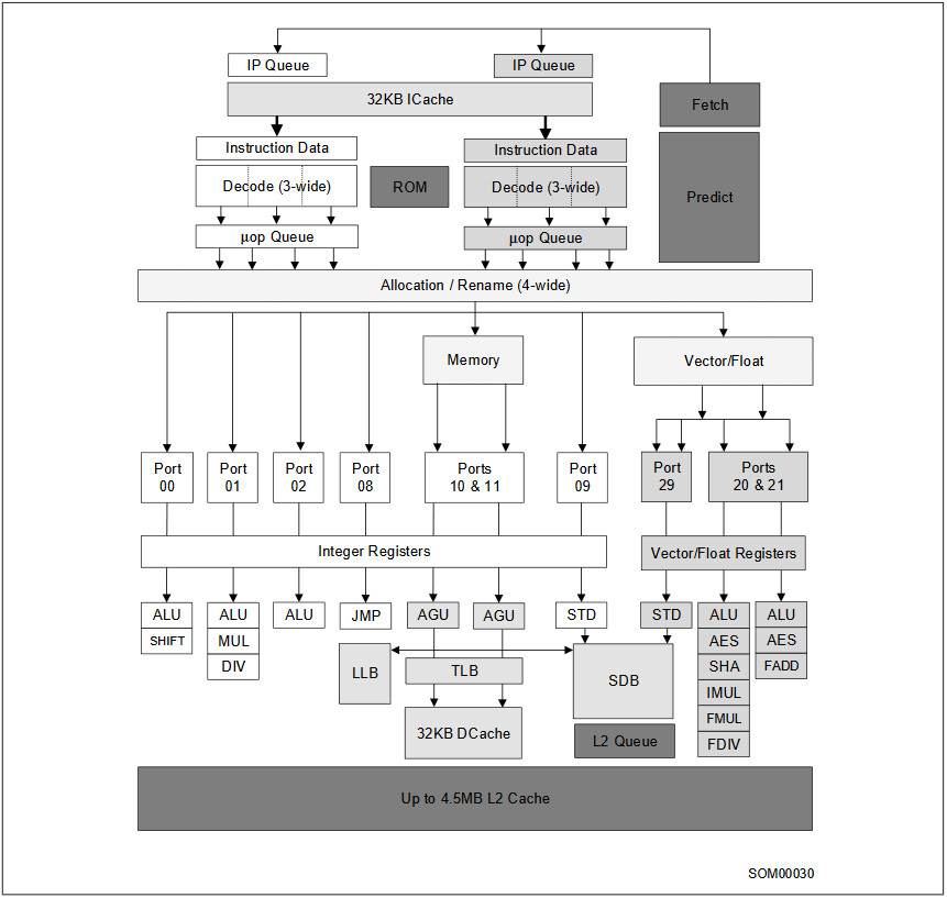
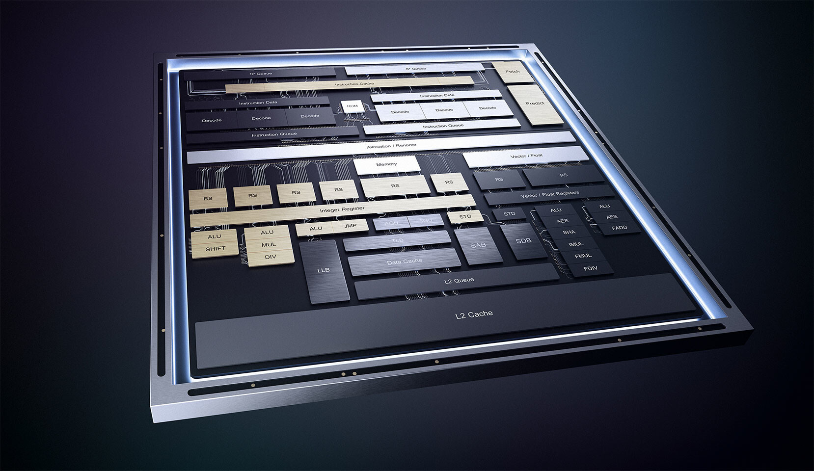
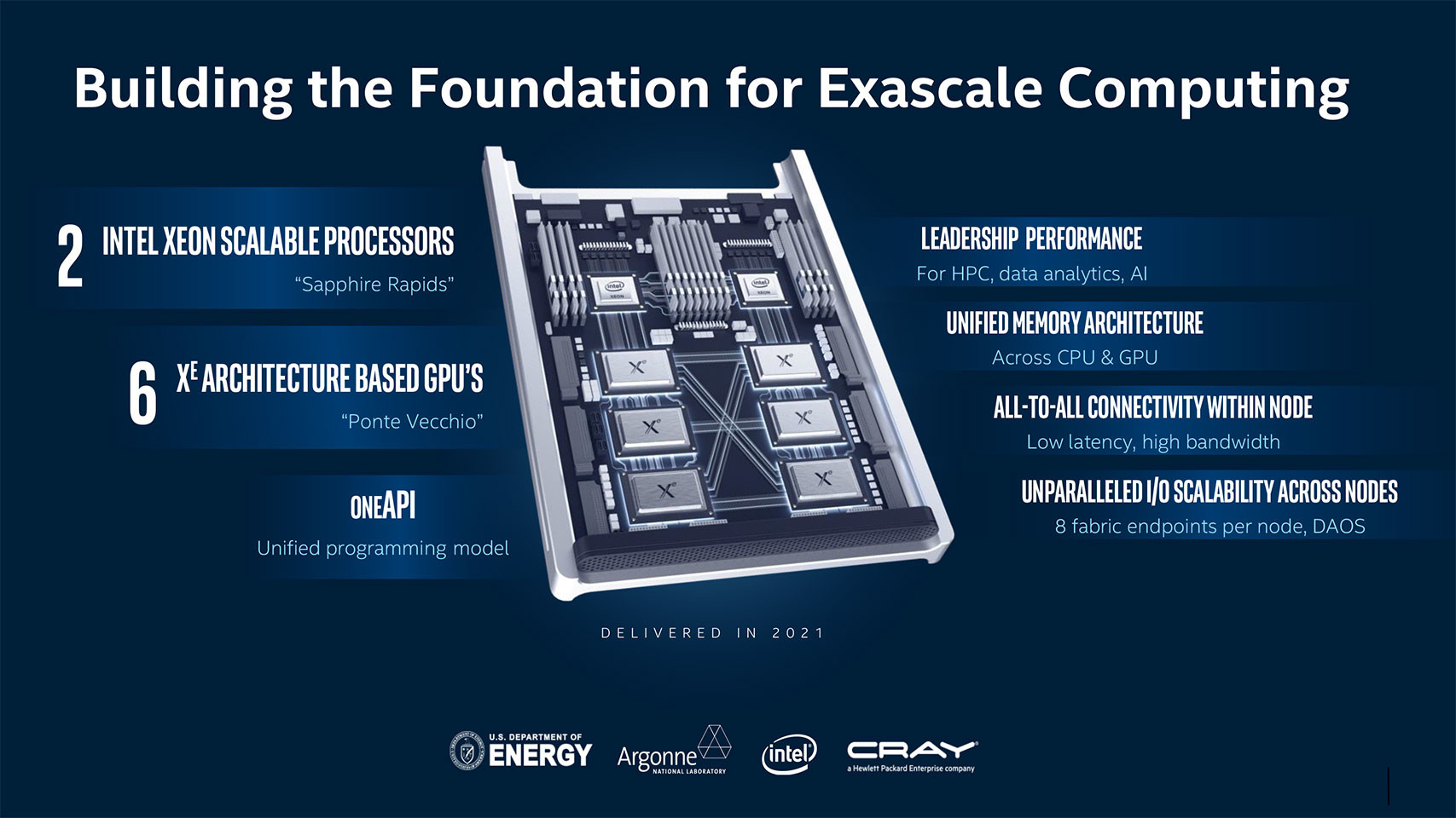
AMD EPYC Scores New Supercomputing and High-Performance Cloud Computing System Wins

AMD today announced multiple new high-performance computing wins for AMD EPYC processors, including that the seventh fastest supercomputer in the world and four of the 50 highest-performance systems on the bi-annual TOP500 list are now powered by AMD. Momentum for AMD EPYC processors in advanced science and health research continues to grow with new installations at Indiana University, Purdue University and CERN as well as high-performance computing (HPC) cloud instances from Amazon Web Services, Google, and Oracle Cloud.

"The leading HPC institutions are increasingly leveraging the power of 2nd Gen AMD EPYC processors to enable cutting-edge research that addresses the world's greatest challenges," said Forrest Norrod, senior vice president and general manager, data center and embedded systems group, AMD. "Our AMD EPYC CPUs, Radeon Instinct accelerators and open software programming environment are helping to advance the industry towards exascale-class computing, and we are proud to strengthen the global HPC ecosystem through our support of the top supercomputing clusters and cloud computing environments."

Apple to Announce its own Mac Processor at WWDC (Late June)

Apple is planning to launch its own high-performance processors designed for Macs at the 2020 WWDC, held in the week of 22 June, 2020. This would be the the first step among many toward the replacement of Intel processors and the x86 machine architecture from the Apple Mac ecosystem, in the same fashion as the company replaced PowerPC with x86 last decade. Apple has codenamed the process of graduating to the new machine architecture "Kalamata," and besides detailing the new processor and its architecture, the company could announce a large-scale developer support initiative to help Mac software vendors to transition to the new architecture in time for the first Macs with the new processors to roll out in 2021.

A Bloomberg report on the new processors states that the chips will be based on the "same technology" as the company's A-series SoCs for iOS devices, meaning that Apple will leverage the Arm machine architecture, and has probably developed a high performance CPU core that can match Intel's x64 cores in IPC and efficiency. Macs based on the new processors, will however run MacOS and not iOS, which means much of the clean-break transition woes between PPC and x86 Macs are bound to return, but probably better managed by software vendors. It also remains to be seen how Apple handles graphics. The company could scale up the Metal-optimized iGPU found in its A-series SoCs on its new Mac processor, while also giving them the platform I/O capability to support discrete graphics from companies such as AMD.

2nd Gen AMD EPYC Processors Now Delivering More Computing Power to Amazon Web Services Customers

AMD today announced that 2nd Gen AMD EPYC processor powered Amazon Elastic Compute Cloud (EC2) C5a instances are now generally available in the AWS U.S. East, AWS U.S. West, AWS Europe and AWS Asia Pacific regions.

Powered by a 2nd Gen AMD EPYC processor running at frequencies up to 3.3Ghz, the Amazon EC2 C5a instances are the sixth instance family at AWS powered by AMD EPYC processors. By using the 2nd Gen AMD EPYC processor, the C5a instance delivers leadership x86 price-performance for a broad set of compute-intensive workloads including batch processing, distributed analytics, data transformations, log analytics and web applications.

Intel Scores Another AMD Graphics Higher-up: Ali Ibrahim

To support its efforts to build a competitive consumer GPU lineup under the Xe brand, which Intel likes to call its "Odyssey," the company scored another higher-up from AMD, this time Ali Ibrahim. He joined Intel this month as a vice-president within the Architecture, Graphics and Software group, although the company didn't specify his responsibilities. "We are thrilled that Ali has joined Intel as Vice President, Platform Architecture and Engineering - dGPUs to be part of the exciting Intel Xe graphics journey," said an Intel spokesperson in a comment to CRN.

During his 13-year tenure at AMD, Ali Ibrahim was the chief-architect of the company's cloud gaming and console SoC businesses, which provides valuable insight into Intel's breakneck efforts to build high-end discrete GPUs (something it lacked for the past two decades). Intel is the only other company that is capable of building semi-custom chips for someone like Microsoft or Sony as the inventor of x86, provided it has a GPU that can match AMD's in the console space. Likewise, with gaming taking baby steps to the cloud as big players such as Google betting on it, Intel sees an opportunity for cloud gaming GPUs that aren't too different from its "Ponte Vecchio" scalar processors. The transfer of talent isn't one-way, as AMD recently bagged Intel's server processor lead Dan McNamara to head the EPYC brand.

Intel Updates x86/x64 Software Developer Manual With Tremont Architecture Details

Intel has today released the 43rd edition of its x86/x64 ISA developer manual designed to help developers see what's new in x86 world and make software optimizations for Intel's platform. In the latest edition of the manual, Intel has revealed the details of its low-power x86 "Tremont" architecture designed for 10 nm efficient, low-power computing. Announced last year in October, Intel promised to deliver a big IPC increase compared to the previous generation low-power CPU microarchitecture like the Goldmont Plus family. To achieve extra performance, Intel has implemented a lot of new solutions.

For starters, Tremont boasts better branch prediction unit, with increased capacity for instruction queue and better path-based conditional and indirect prediction. The front-end fetch and decode pipeline have been updated as well. Now the design is a 6-wide Out of Order Execution (OoOE) pipeline which can process 6 instructions per cycle. The Data cache is now upgraded to 32 KB. The load and store execution pipelines are now doubled and they are capable of two loads and two stores, or one load and one store, depending on the application. Tremont also updates on one important point and that is a dedicated store data port for integer and vector integer/floating-point data. Another big improvement is happening in the cryptography department. Tremont now features Galois-field instructions labeled as the GFNI family of instructions. There are two AES units for faster AES encryption and decryption. The already implemented SHA-NI cryptography standard was enhanced and it now is much faster as well. For mode in-depth report please check out Intel's x86/x64 manual.
Intel Tremont

Intel Jasper Lake CPU Appears with Gen11 Graphics

Intel is preparing to update its low-end segment designed for embedded solutions, with a next-generation CPU codenamed Jasper Lake. Thanks to the popular hardware finder and leaker, _rogame has found a benchmark showing that Intel is about to bless low-end with a lot of neat stuff. The benchmark results show a four-core, four threaded CPU running at 1.1 GHz base clock with a 1.12 GHz boost clock. Even though these clocks are low, this is only a sample and the actual frequency will be much higher, expecting to be near 3 GHz. The CPU was spotted in a configuration rocking 32 GB of DDR4 SODIMM memory.

Jasper Lake is meant to be a successor to Gemini Lake and it will use Intel's Tremont CPU architecture designed for low-power scenarios. Designed on a 10 nm manufacturing node from Intel, this CPU should bring x86 processors to a wide range of embedded systems. Although the benchmark didn't mention which graphics the CPU will be paired with, _rogame speculates that Intel will use Gen11 graphics IP. That will bring a nice update over Gemini Lake's Gen9.5 graphics. That alone should bring better display output options and more speed. These CPUs are designed for Atom/Pentium/Celeron lineup, just like Gemini Lake before them.

Update: Updated the article to reflect the targeted CPU category.
Intel Tremont Intel Jasper Lake

Intel Apparently Reserving 28 W Ice Lake Mobile Chips for Apple, Removes Entries from ARK

The idea of an ARK is to preserve that which enters it; however, the legend on the basis of arks and their concept must've slipped Intel's internal memos. The company has de-listed a previously detailed Ice Lake mobile CPU from its database - the Core i7-1068G7 - which was a 28 W part available for system integrators to build machines around. That part was special, because it was - then - the only 28 W part listed for mobile Ice Lake, with the rest of the CPU lineup having configurable TDPs between 12 W and 25 W - thus having a lesser maximum theoretical performance due to reduced TDP.

In its stead, Intel has entered a new, Core i7-1068NG7 (yes, the same naming with an extra N), which places this as an Apple-exclusive CPU, according to the folks over at Notebookcheck. Besides this entry, Intel has also listed the i5-1038NG7, which also features a 28 W TDP that's higher than the other available CPUs for other system integrators. If this is true, then Intel is reserving its cream-of-the-crop CPUs for Apple. Since the California-based company wouldn't be using parts with worse thermal and power consumption figures than what's available for others, the only answer to how these products came to being is that they are binned CPUs with better than average characteristics. Intel could be doing this to keep Apple happy even as the California-based company is well on its way to eschew its dependence on x86 with a fully internally-developed ARM CPU.

NVIDIA Underestimated AMD's Efficiency Gains from Tapping into TSMC 7nm: Report

A DigiTimes premium report, interpreted by Chiakokhua, aka Retired Engineer, chronicling NVIDIA's move to contract TSMC for 7 nm and 5 nm EUV nodes for GPU manufacturing, made a startling revelation about NVIDIA's recent foundry diversification moves. Back in July 2019, a leading Korean publication confirmed NVIDIA's decision to contract Samsung for its next-generation GPU manufacturing. This was a week before AMD announced its first new-generation 7 nm products built for the TSMC N7 node, "Navi" and "Zen 2." The DigiTimes report reveals that NVIDIA underestimated the efficiency gains AMD would yield from TSMC N7.

With NVIDIA's bonhomie with Samsung underway, and Apple transitioning to TSMC N5, AMD moved in to quickly grab 7 nm-class foundry allocation and gained prominence with the Taiwanese foundry. The report also calls out a possible strategic error on NVIDIA's part. Upon realizing the efficiency gains AMD managed, NVIDIA decided to bet on TSMC again (apparently without withdrawing from its partnership with Samsung), only to find that AMD had secured a big chunk of its nodal allocation needed to support its growth in the x86 processor and discrete GPU markets. NVIDIA has hence decided to leapfrog AMD by adapting its next-generation graphics architectures to TSMC's EUV nodes, namely the N7+ and N5. The report also speaks of NVIDIA using its Samsung foundry allocation as a bargaining chip in price negotiations with TSMC, but with limited success as TSMC established its 7 nm-class industry leadership. As it stands now, NVIDIA may manufacture its 7 nm-class and 5 nm-class GPUs on both TSMC and Samsung.

Intel "Tiger Lake" and "Lakefield" to Launch Around September-October, 2020

The 11th generation Intel Core "Tiger Lake" mobile processor and pioneering "Lakefield" heterogenous x86 processor could debut around September or October, 2020, according to a leaked Lenovo internal slide posted by NotebookCheck. It also points to Intel denoting future processors' lithography with Foveros 3D Packaging as simply "3D," and not get into a nanometer number-game with AMD (which is now in 7 nm and on course to 5 nm in 2022). This makes sense as Foveros allows the combination of dies built on different silicon fabrication nodes.

"Tiger Lake" is still denoted as a 10 nm as it's a planar chip. Intel is developing it on a refined 10 nm+ silicon fabrication process, which apparently enables Intel to increase clock speeds without breaking the target power envelope. "Tiger Lake" sees the commercial debut of Intel's ambitious Xe graphics architecture as an iGPU solution. "Lakefield," on the other hand, is a 5-core processor combining four "Tremont" low power x86-64 cores with a "Sunny Cove" high-powered core, in a setup rivaling Arm big.LITTLE, enabling the next generation of mobile computing form-factors, which Intel and its partners are still figuring out under Project Athena.

Intel's Alder Lake Processors Could use Foveros 3D Stacking and Feature 16 Cores

Intel is preparing lots of interesting designs for the future and it is slowly shaping their vision for the next generation of computing devices. Following the big.LITTLE design principle of Arm, Intel decided to try and build its version using x86-64 cores instead of Arm ones, called Lakefield. And we already have some information about the new Alder Lake CPUs based on Lakefield design that are set to be released in the future. Thanks to a report from Chrome Unboxed, who found the patches submitted to Chromium open-source browser, used as a base for many browsers like Google Chrome and new Microsoft Edge, there is a piece of potential information that suggests Alder Lake CPUs could arrive very soon.

Rumored to feature up to 16 cores, Alder Lake CPUs could present an x86 iteration of the big.LITTLE design, where one pairs eight "big" and eight "small" cores that are activated according to increased or decreased performance requirements, thus bringing the best of both worlds - power efficiency and performance. This design would be present on Intel's 3D packaging technology called Foveros. The Alder Lake CPU support patch was added on April 27th to the Chrome OS repository, which would indicate that Intel will be pushing these CPUs out relatively quickly. The commit message titled "add support for ADL gpiochip" contained the following: "On Alderlake platform, the pinctrl (gpiochip) driver label is "INTC105x:00", hence declare it properly." The Chrome Unboxed speculates that Alder Lake could come out in mid or late 2021, depending on how fast Intel could supply OEMs with enough volume.
Intel Lakefield

Apple to Launch Arm-Powered MacBook in the next 18 Months

Apple is currently designing a custom series of CPUs, for its Macbook laptop lineup, based on the Arm Instruction Set Architecture. Having designed some of the most powerful mobile processors that are inside the iPhone series of devices, Apple is preparing to make a jump to an even more powerful device lineup by bringing custom CPUs for MacBook. Tired of the speed by which Intel replaces and upgrades its Core lineup of CPUs, Apple decided to take the matter in its own hands and rumors about the switch to a custom solution have been going on for a while. However, we now have some information about when to expect the first wave of Arm-powered Macs.

According to the analyst Ming-Chi Kuo, who is a well-known insider in the Apple industry, we can expect the first wave of the Arm-powered Macbook in the next 18 months, precisely in the first half of 2021. Supposedly, the first chips for these new Macs are going to be manufactured on a 5 nm manufacturing process, possibly over at TSMC since Apple had a long-lasting history of manufacturing its chips at TSMC foundries. In the meantime, we can expect to see Apple providing developers with tools to transition their x86-64 software to the new Arm ISA. Without a software ecosystem, the hardware platform is essentially worthless. And Apple knows this. We will see how they plan to play it and will report as soon as there is more information.

VIA CenTaur CHA NCORE AI CPU Pictured, a Socketed LGA Package

VIA's CenTaur division sprung an unexpected surprise in the CPU industry with its new CHA x86-64 microarchitecture and an on-die NCORE AI co-processor. This would be the first globally-targeted x86 processor launch by a company other than Intel and AMD in close to 7 years, and VIA's first socketed processor in over 15 years. SemiAccurate scored a look at mock-up of the CenTaur CHA NCORE 8-core processor and it turns out that the chip is indeed socketed.

Pictured below, the processor is a flip-chip LGA. We deduce it is socketed looking at its alignment notches and traces for ancillaries on the reverse-side (something BGAs tend to lack). On the other hand, the "contact points" of the package appear to cast shadows, and resemble balls on a BGA package. Topside, we see an integrated heatspreader (IHS), and underneath is a single square die. CenTaur built the CHA NCORE on TSMC's 16 nm FinFET process. The package appears to have quite a high pin-count for a die this size, but that's probably because of its HEDT-rivaling I/O, which includes a quad-channel DDR4 memory interface and 44 PCI-Express gen 3.0 lanes.

Microsoft Enables Hyper-V Support for Windows-on-ARM Devices

Microsoft is determined in its goal to move away from x86-64 dominance it had in the personal computer space for many decades. In the latest Windows 10 Insider Preview Build 19559, Microsoft has enabled Hyper-V support for ARM64 devices, such as Surface Pro X. Hyper-V is a Windows native hypervisor and it is Microsoft's virtualization technology that allows running other OSes on top of Windows. Being a low-overhead solution, it is more efficient than a virtual machine and allows for better performance of OS that is running on top of Windows.

With the Insider Preview Build 19559, Microsoft is enabling this feature on a Windows 10 Pro and Windows 10 Enterprise customers. It is important to note that by adding more features like this, Microsoft is expanding the software ecosystem of ARM64 devices, which should result in wider adoption of PCs like the Surface Pro X.

AMD Desktop Processor Market Share Now at 18.3%: Mercury Research

Market intelligence firm Mercury Research published its findings on the x86 processor market towards the end of 2019, in which AMD has posted growth in all segments (not counting IoT or semi-custom). AMD held 18.3 percent of the desktop x86 processor market, according to the report. a 5-year high. The company's EPYC line of server processors face a more uphill battle against enterprises' entrenched brand loyalties to Intel. The company holds 4.5 percent of the server processor market, but growing 0.2 percent points versus the previous quarter, and 1.4 percentage points vs. the previous year. The last time AMD held such a market share in the server x86 processor market was in Q3-2013.

AMD's mobile processor market share may come as a surprise to some. According to Mercury Research, the company holds 16.2 percent of the mobile x86 processor market, which is almost as much as its desktop market. This is probably propelled by the popularity of AMD APUs and low-power CPUs in the cost-effective notebook market segments. AMD is now eyeing higher market segments with its Ryzen 4000 "Renoir" processors that make landfall this year. AMD is growing faster in the mobile space than desktop, with 1.5 percentage points growth in just Q4, and 4 percentage points year-over-year. AMD's mobile market share was this high back in Q2-2013. Mercury Research pins AMD's overall hold over the x86 market at 15.5%, averaged on all segments, minus semi-custom and IoT.

Zhaoxin KaiXian x86 Processor Now Commercially Available to the DIY Channel

Zhaoxin is a brand that makes multi-core 64-bit x86 processors primarily for use in Chinese state IT infrastructure. It's part of the Chinese Government's ambitious plan to make its IT hardware completely indigenous. Zhaoxin's x86-64 CPU cores are co-developed by licensee VIA, specifically its CenTaur subsidiary that's making NCORE AI-enabled x86 processors. The company's KaiXian KX-6780A processor is now commercially available in China to the DIY market in the form of motherboards with embedded processors.

The KaiXian KX-6780A features an 8-core/8-thread x86-64 CPU clocked up to 2.70 GHz, 8 MB of last-level cache, a dual-channel DDR4-3200 integrated memory controller, a PCI-Express gen 3.0 root-complex, and an iGPU possibly designed by VIA's S3 Graphics division, which supports basic display and DirectX 11.1 readiness. The CPU features modern ISA, with instruction sets that include AVX, AES-NI, SHA-NI, and VT-x comparable virtualization extensions. The chip has been fabricated on TSMC 16 nm FinFET process.

Intel Core i5-L16G7 is the first "Lakefield" SKU Appearance, Possible Prelude to New Nomenclature?

Intel Core i5-L16G7 is the first commercial SKU that implements Intel's "Lakefield" heterogenous x86 processor architecture. This 5-core chip features one high-performance "Sunny Cove" CPU core, and four smaller "Tremont" low-power cores, with an intelligent scheduler balancing workloads between the two core types. This is essentially similar to ARM big.LITTLE. The idea being that the device idles most of the time, when lower-powered CPU cores can hold the fort; performance cores kick in only when really needed, until which time they remain power-gated. Thai PC enthusiast TUM_APISAK discovered the first public appearance of the i5-L16G7 in an unreleased Samsung device that has the Userbenchmark device ID string "SAMSUNG_NP_767XCL."

Clock speeds of the processor are listed as "1.40 GHz base, with 1.75 GHz turbo," but it's possible that the two core types have different clock-speed bands, just like the cores on big.LITTLE SoCs. Other key components of "Lakefield" include an iGPU based on the Gen11 graphics architecture, and an LPDDR4X memory controller. "Lakefield" implements Foveros packaging, in which high-density component dies based on newer silicon fabrication nodes are integrated with silicon interposers based on older fabrication processes, which facilitate microscopic high-density wiring between the dies. In case of "Lakefield," the Foveros package features a 10 nm "compute field" die sitting atop a 22 nm "base field" interposer.

VIA CenTaur Develops a Multi-core x86 Processor for Enterprise with in-built AI Hardware

Tasting Intel's blood in the water with AMD's return to competitiveness, dormant x86 licensee VIA wants to take another swing at the market, this time with a multi-core processor targeted at enterprises and possibly workstations, developed by its subsidiary CenTaur. The company appears to want to cash in on the AI boom, and could develop turnkey facial-recognition CCTV solutions with the chip. CenTaur is ready with a working prototype. It features eight 64-bit x86 CPU cores, and an on-die "AI co-processor" named NCORE. A ringbus connects the eight CPU cores and the NCORE with the processor's other components. The processor features 16 MB of shared L3 cache, a quad-channel DDR4-3200 memory interface, and a 44-lane PCI-Express gen 3.0 root-complex, along with a fully integrated southbridge, making it an SoC. It also appears to be multi-socket capable, although VIA didn't detail the interconnect in use.

The NCORE is a PCI-mapped device to the software, which provides functions such as DNN building and training acceleration. From the looks of it, there's more to NCORE than simply a fixed-function hardware that multiplies matrices. Its developers state that the device accelerates AI at a rate of "20 trillion AI operations/sec with 20 terabytes/sec memory bandwidth." The CPU cores on the processor tick at 2.50 GHz, and while VIA hasn't made any IPC claims, it has mentioned support for the cutting-edge AVX-512 instruction-set, something even "Zen 2" lacks, which possibly indicates a powerful FPU. The silicon measures 195 mm², and has been built on 16 nm FinFET node at TSMC. VIA will demonstrate the unnamed processor and its testbed at ISC East 2019, held on November 20 and 21.

The full technology announcement slide-deck follows.

Intel Announces New GPU Architecture and oneAPI for Unified Software Stack at SC19

At Supercomputing 2019, Intel unveiled its vision for extending its leadership in the convergence of high-performance computing (HPC) and artificial intelligence (AI) with new additions to its data-centric silicon portfolio and an ambitious new software initiative that represents a paradigm shift from today's single-architecture, single-vendor programming models.

Addressing the increasing use of heterogeneous architectures in high-performance computing, Intel expanded on its existing technology portfolio to move, store and process data more effectively by announcing a new category of discrete general-purpose GPUs optimized for AI and HPC convergence. Intel also launched the oneAPI industry initiative to deliver a unified and simplified programming model for application development across heterogenous processing architectures, including CPUs, GPUs, FPGAs and other accelerators. The launch of oneAPI represents millions of Intel engineering hours in software development and marks a game-changing evolution from today's limiting, proprietary programming approaches to an open standards-based model for cross-architecture developer engagement and innovation.

Microsoft Could Bring x86-64 App Emulation to Windows on ARM

According to the sources close to Neowin, Microsoft is expected to launch x86-64 (or x64 in short) emulation support for Windows on ARM (WoA) devices. Expected to arrive in Windows 10 21H1, or around 2020 for all the Windows Insiders, the new feature will enable a vast majority of apps made for Windows OS, currently built for x64 architecture, to run on ARM ISA and all Windows on ARM computers.

So far, only 32-bit x86 applications were able to be emulated, however, if these rumors are to be believed, many users of WoA devices should get a chance to run all of their favorite 64-bit software that was previously unavailable. The launch of this feature will boost the adoption of the WoA ecosystem with benefits reaching all existing laptop models, including Microsoft's newly launched Surface Pro X laptop that utilizes an ARM-based chip called SQ1 (customized Qualcomm Snapdragon 8cx processor).

G.SKILL Memory First to Break DDR4 6 GHz World Record Speed

G.SKILL, the world's leading manufacturer of extreme performance memory and gaming peripherals, is very thrilled to announce a new world record for the fastest memory frequency at DDR4-6016.8 MHz, being the first ever to break through the DDR4-6000 barrier. This milestone is set by the Taiwanese professional overclocker, TopPC, using G.SKILL DDR4 Trident Z Royal memory on the latest MSI MPG Z390I GAMING EDGE AC motherboard and Intel Core i9-9900K processor.

Just 3 short months after the world record DDR4-5886MHz set by Toppc at the G.SKILL Computex booth in June, Toppc has once again set a new world record for memory frequency speed and is the first to push DDR4 memory to an astonishing 6 GHz. The validation links for this major milestone can be found in the following CPU-Z validation link and HWBot website screenshot below (validation).

AMD Designing Zen 4 for 2021, Zen 3 Completes Design Phase, out in 2020

AMD in its 2nd generation EPYC processor launch event announced that it has completed the design phase of its next-generation "Zen 3" CPU microarchitecture, and is currently working on its successor, the "Zen 4." AMD debuted its "Zen 2" microarchitecture with the client-segment 3rd generation Ryzen desktop processor family, it made its enterprise debut with the 2nd generation EPYC. This is the first x86 CPU microarchitecture designed for the 7 nanometer silicon fabrication process, and is being built on a 7 nm DUV (deep ultraviolet) node at TSMC. It brings about double-digit percentage IPC improvements over "Zen+."

The "Zen 3" microarchitecture is designed for the next big process technology change within 7 nm, EUV (extreme ultraviolet), which allows significant increases in transistor densities, and could facilitate big improvements in energy-efficiency that could be leveraged to increase clock-speeds and performance. It could also feature new ISA instruction-sets. With "Zen 3" passing design phase, AMD will work on prototyping and testing it. The first "Zen 3" products could debut in 2020. "Zen 4" is being designed for a different era.

Next-generation Intel Xeon Scalable Processors to Deliver Breakthrough Platform Performance with up to 56 Processor Cores

Intel today announced its future Intel Xeon Scalable processor family (codename Cooper Lake) will offer customers up to 56 processor cores per socket and built-in AI training acceleration in a standard, socketed CPU as part of its mainline Intel Xeon Scalable platforms, with availability in the first half of 2020. The breakthrough platform performance delivered within the high-core-count Cooper Lake processors will leverage the capabilities built into the Intel Xeon Platinum 9200 series, which today is gaining momentum among the world's most demanding HPC customers, including HLRN, Advania, 4Paradigm, and others.

"The Intel Xeon Platinum 9200 series that we introduced as part of our 2nd Generation Intel Xeon Scalable processor family generated a lot of excitement among our customers who are deploying the technology to run their high-performance computing (HPC), advanced analytics, artificial intelligence and high-density infrastructure. Extended 56-core processor offerings into our mainline Intel Xeon Scalable platforms enables us to serve a much broader range of customers who hunger for more processor performance and memory bandwidth."
-Lisa Spelman, vice president and general manager of Data Center Marketing, Intel Corporation

Intel Starts Shipping 10 nm Ice Lake CPUs to OEMs

During its second quarter earnings call, Intel announced that it has started shipping of 10th generation "Core" CPUs to OEMs. Making use of 10 nm lithography, the 10th generation of "Core" CPUs, codenamed Ice Lake, were qualified by OEMs earlier in 2019 in order to be integrated into future products. Ice Lake is on track for holiday season 2019, meaning that we can expect products on-shelves by the end of this year. That is exciting news as the 10th generation of Core CPUs is bringing some exciting micro-architectural improvements along with the long awaited and delayed Intel's 10nm manufacturing process node.

The new CPUs are supposed to get around 18% IPC improvement on average when looking at direct comparison to previous generation of Intel CPUs, while being clocked at same frequency. This time, even regular mobile/desktop parts will get AVX512 support, alongside VNNI and Cryptography ISA extensions that are supposed to bring additional security and performance for the ever increasing number of tasks, especially new ones like Neural Network processing. Core configurations will be ranging from dual core i3 to quad core i7, where we will see total of 11 models available.

AMD Halts Further x86 Technology Licensing to China

AMD Lisa Su at Computex 2019 confirmed to Tom's hardware that the company wasn't licensing anymore of its x86 IP portfolio to China-based companies. AMD entered a technology license agreement with China's Tianjin Haiguang Advanced Technology Investment Co. Ltd. (THATIC) in 2016. As part of the agreement to license its x86 and SoC IP for chip development, AMD received a cash infusion worth $293 million (plus royalties).

As a result, Chinese chipmaker Hygon started delivering their "Dhyana" CPUs, which looked like copies of AMD's Zen-based Epyc chips with added, Chinese-government approved cryptographic capabilities. AMD had to go through some hoops to get this deal done, but it did. However, now the technology refinement pipe is draining for the Chinese companies, as AMD won't be delivering its post-Zen updates to the core design. It remains to be seen if AMD's intellectual property was enough for Chinese companies to ignite their own in-country CPU development, or if the ongoing US-China trade war will keep on draining the company of CPU independence.

Intel Releases ModernFW as Open Source, minimal Firmware Replacement

Today Intel announced ModernFW - an experimental approach to building a minimum viable platform firmware for machines such as cloud server platforms. The reason for this software is that, while traditional PC Firmware has evolved over time and retained its backward compatibility, it has become very big and often inefficient.

So to meet the requirements of new platforms that need to be built quickly and adapted easily, Intel decided to offer a new software package that will help with that. The new firmware package targets x86_64 from ISA standpoint and Linux kernel based OSes.
Return to Keyword Browsing
May 10th, 2024 18:42 EDT change timezone

New Forum Posts

Popular Reviews

Controversial News Posts