Thursday, January 21st 2016

First 10 nm Intel Processor Out in 2017

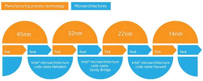
With Intel's "tick-tock" product development cycle slowing down to a 3-launch cadence per silicon fab process, the company is preparing to launch no less than three micro-architectures on its next 10 nanometer silicon fab process. The first 10 nm CPU by Intel will launch in 2017.

In 2016, Intel will launch its 7th generation Core "Kaby Lake" processor, its third chip on the 14 nm process (after "Broadwell" and "Skylake"). The first 10 nm micro-architecture will be codenamed "Cannonlake," and will launch some time in 2017. Intel will build chips on the 10 nm for two more generations after "Cannonlake." The company's 2018 micro-architecture, built on the 10 nm will be codenamed "Icelake," and its 2019 release will be codenamed "Tigerlake." It's only 2020 that the company will pull out its next silicon fab process, 5 nm.
Source: OC3D
Add your own comment

29 Comments on First 10 nm Intel Processor Out in 2017

#1
buggalugs
So its more like a tick, tock, tock from now on?? Whats after 5 nm?
Posted on Reply
#2
Frick
Fishfaced Nincompoop
I don't believe they'll make it to 5nm by 2020.
Posted on Reply
#3
dj-electric
Keep slowing down intel, we currently need you to do it.... kinda.
Posted on Reply
#4
RejZoR
buggalugsSo its more like a tick, tock, tock from now on?? Whats after 5 nm?
tock tock tock tock XD
Posted on Reply
#5
R-T-B
RejZoRtock tock tock tock XD
I think this clock is broken.
Posted on Reply
#8
Chaitanya
So it's a desperate search for viable alternative to Silicon for electronics.
Posted on Reply
#9
Assimilator
FrickI don't believe they'll make it to 5nm by 2020.
If TSMC thinks they can, Intel definitely can.
ChaitanyaSo it's a desperate search for viable alternative to Silicon for electronics.
Hardly desperate. The big names in the industry (Intel, IBM, et cetera) have been working on post-silicon technologies for years, there just hasn't been any economic reason to promote said technologies to mainstream because silicon is a cheap and known quantity. But by the time silicon is no longer feasible, you can bet the farm that all the fabbing companies will have switched to a replacement.
Posted on Reply
#10
MIRTAZAPINE
10nm! That is smaller than high ultraviolet wavelengths! It approaching the size of atoms can't believe I would witness this in my lifetime. This will be very very hard. Perhaps the move after silicon is carbon nanotubes and maybe biological computers? I think most like cpu will be build in a 3d plane now since silicon is nearing the end. Not intel trigate but building it up like building with multiple floors
R-T-BI think it's probably cheaper to just bend the fabric of time to match the clocks new "tick-tock"
It'll be more expensive we hardly build rockets able to travel the speed of light and the hadron collider is damn expensive. There is not enough mini blackhole created by them. :p
Posted on Reply
#11
Prima.Vera
Good. Cannot wait for 1nm tech and under.
Posted on Reply
#12
64K
I doubt that 5nm will be on silicon considering the problems Intel is having just getting to 10nm with silicon. The next step after 10nm will most likely be on a different material that will allow for large increases in GHz for the same watts or the same performance as Cannonlake/ Icelake/ Tigerlake mobile CPUs for a lot less watts and longer battery life. 2020 doesn't seem unreasonable to me to make this happen but we'll see.
Posted on Reply
#13
Sasqui
buggalugsSo its more like a tick, tock, tock from now on?? Whats after 5 nm?
An article I read (which I can't find) said the Fin Fet (3D transistors) simply won't work below 10nm they way they are currently designed, so they're going to either go with a new type of transistor or turn to all the mice on earth to solve the problem of the question to the number 42.
Posted on Reply
#14
yogurt_21
Prima.VeraGood. Cannot wait for 1nm tech and under.
ah yes picometer territory 1000pm = 1 nm

Considering that certain atoms are half a nanometer (500pm) in diameter it is difficult to see us getting that far down anytime soon. Subatomic processors don't seem to be reality just yet.
Posted on Reply
#15
wolar
buggalugsSo its more like a tick, tock, tock from now on?? Whats after 5 nm?
I think the they reach the hardware limitation , 10-8nm if i remember correctly is the lowest they can go due to the hardware they are using , after they reached that they will move on to different hardware(or finding new ways to make the processors faster with keeping the 8nm die) , which will be some true upgrade i expect.
Posted on Reply
#16
TheGuruStud
Given the naming convention, it's safe to say that nothing is changing. I can't wait for sandy bridge v10!
Posted on Reply
#17
bubbleawsome
buggalugsSo its more like a tick, tock, tock from now on?? Whats after 5 nm?
With the smaller bits I think it's more tock, tick, tick :P
Posted on Reply
#18
alucasa
Kinda excited to see what will come as silicon replacement.
Posted on Reply
#19
HumanSmoke
64KI doubt that 5nm will be on silicon considering the problems Intel is having just getting to 10nm with silicon. The next step after 10nm will most likely be on a different material that will allow for large increases in GHz for the same watts or the same performance as Cannonlake/ Icelake/ Tigerlake mobile CPUs for a lot less watts and longer battery life. 2020 doesn't seem unreasonable to me to make this happen but we'll see.
Sorry to blow your theory out of the water but 10nm (and it's half-node successor 7nm for Samsung/TSMC) as well as 5nm have been confirmed for conventional FinFET manufacture. The big question was the lithography, which was clarified with ASML's product roadmap (and all but confirmed by Intel's and TSMC's orders) back in September, and the tape out of the first 5nm test chips a few months ago. The big issue is cost and availability. ASML's NXE:3400B litho tool was pegged at $US120 million per system by ASML back in September. Given that ASML delivers less than one system per month and Intel's orders alone equal or surpass that total you could see that Intel, TSMC, Samsung, Intel, UMC, and Glofo's principle bottleneck aside from pricing would be getting their hands on deliveries. The other principle area of concern (aside from fab retooling) was the prodigious power usage of litho lasers. Watts-per-wafer is a pretty important metric in lithography.

To anyone with an interest in the process tech, I'd suggest a browse of ASML's presentation for the coming year (PDF). It only covers 10nm/7nm since the 3400B won't come online until late in the year.
Posted on Reply
#20
[502]
I don't know what to say. Not too many years ago (2005 methinks) I still using 130nm processors, and here we are now, about twelve years later we're gonna have 10nm processors.
Maybe it's true that Skynet has begin to operate.
Posted on Reply
#21
64K
HumanSmokeSorry to blow your theory out of the water but 10nm (and it's half-node successor 7nm for Samsung/TSMC) as well as 5nm have been confirmed for conventional FinFET manufacture. The big question was the lithography, which was clarified with ASML's product roadmap (and all but confirmed by Intel's and TSMC's orders) back in September, and the tape out of the first 5nm test chips a few months ago. The big issue is cost and availability. ASML's NXE:3400B litho tool was pegged at $US120 million per system by ASML back in September. Given that ASML delivers less than one system per month and Intel's orders alone equal or surpass that total you could see that Intel, TSMC, Samsung, Intel, UMC, and Glofo's principle bottleneck aside from pricing would be getting their hands on deliveries. The other principle area of concern (aside from fab retooling) was the prodigious power usage of litho lasers. Watts-per-wafer is a pretty important metric in lithography.

To anyone with an interest in the process tech, I'd suggest a browse of ASML's presentation for the coming year (PDF). It only covers 10nm/7nm since the 3400B won't come online until late in the year.
I guess things have changed. I was going from this article

arstechnica.com/gadgets/2015/02/intel-forges-ahead-to-10nm-will-move-away-from-silicon-at-7nm/

granted it is almost a year old.
Posted on Reply
#22
HumanSmoke
[502]I don't know what to say. Not too many years ago (2005 methinks) I still using 130nm processors, and here we are now, about twelve years later we're gonna have 10nm processors.
Maybe it's true that Skynet has begin to operate.
The time frame would be a little longer than that. 130nm dates from 2001-02 (Intel's Pentium III Tualatin and AMD's Athlon XP Thoroughbred). 90nm arrived in 2004. By 2005 Intel was on their 65nm P1264 process, AMD was still on 90nm SOI until mid 2006, as were TSMC (CLN90GT).
64KI guess things have changed. I was going from this article

arstechnica.com/gadgets/2015/02/intel-forges-ahead-to-10nm-will-move-away-from-silicon-at-7nm/

granted it is almost a year old.
Yes, I think up until comparatively recently, it was thought that EUV wouldn't scale to 5nm, but it seems where needs must they have managed to make it workable. 3nm is going to be a bridge too far for EUV by the sounds of it, but at least the process guys have a decade or more to tackle that problem of making 3nm commercially viable.
Posted on Reply
#23
bug
buggalugsSo its more like a tick, tock, tock from now on?? Whats after 5 nm?
5nm is awfully close to the physical limitations of silicon (some place that limit at 7-8nm). So whatever comes after 5nm will almost certainly be not-silicon.
Posted on Reply
#24
citizenzero
buggalugsSo its more like a tick, tock, tock from now on?? Whats after 5 nm?
It's more like snap crackle pop
Posted on Reply
#25
peche
Thermaltake fanboy
CanonLake and 200 series chipset.... 2017....{union point} interesting .. hoping there wont be a half die iGPU and more GHZ on that chip...
Kabylake = Skylake refresh
5nm well, hard to believe..
Posted on Reply
Add your own comment
Apr 25th, 2024 20:43 EDT change timezone

New Forum Posts

Popular Reviews

Controversial News Posts