Thursday, March 7th 2019

Toshiba and Western Digital Readying 128-layer 3D NAND Flash
Toshiba and its strategic ally Western Digital are readying a high-density 128-layer 3D NAND flash memory. In Toshiba's nomenclature, the chip will be named BiCS-5. Interestingly, despite the spatial density, the chip will implement TLC (3 bits per cell), and not the newer QLC (4 bits per cell). This is probably because NAND flash makers are still spooked about the low yields of QLC chips. Regardless, the chip has a data density of 512 Gb. With 33% more capacity than 96-layer chips, the new 128-layer chips could hit commercial production in 2020-21.
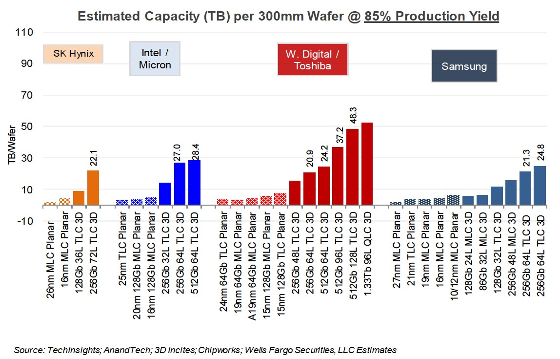
The BiCS-5 chip reportedly features a 4-plane design. Its die is divided into four sections, or planes, which can each be independently accessed; as opposed to BiCS-4 chips that use a 2-plane layout. This reportedly doubles the write performance per unit-channel to 132 MB/s from 66 MB/s. The die also reportedly uses CuA (circuitry under array), a design innovation in which logic circuitry is located in the bottom-most "layer," with data layers stacked above, resulting in 15 percent die-size savings. Aaron Rakers, a high-technology industry market analyst with Wells Fargo, estimates that Toshiba-WD's yields per 300 mm wafer could be as high as 85 percent.


Source:
Blocks & Files
The BiCS-5 chip reportedly features a 4-plane design. Its die is divided into four sections, or planes, which can each be independently accessed; as opposed to BiCS-4 chips that use a 2-plane layout. This reportedly doubles the write performance per unit-channel to 132 MB/s from 66 MB/s. The die also reportedly uses CuA (circuitry under array), a design innovation in which logic circuitry is located in the bottom-most "layer," with data layers stacked above, resulting in 15 percent die-size savings. Aaron Rakers, a high-technology industry market analyst with Wells Fargo, estimates that Toshiba-WD's yields per 300 mm wafer could be as high as 85 percent.


4 Comments on Toshiba and Western Digital Readying 128-layer 3D NAND Flash
Those graphs are also a bit misleading... 96L TLC numbers for the other manufacturers aren't included, and if you compare the most common listed flash between all of them (256Gb TLC), WD/Toshiba actually comes in last in TB/wafer, which means that the other manufacturers' yields on 128L should be still higher. That said, WD/Toshiba were the first to market with a 96L product in November last year already, while the others have announced they have 96L flash but haven't yet shipped 96L products.
Also, look at those MLC TB/wafer figures compared to TLC, holy hell.
Is QLC NAND Flash produced separately? Cannot it just binned from the same dies?The graph is not yields (it's given at iso-85% yield rate) but density. 256Gb TLC seems to be the only reasonable comparison point:
22.1 - SK Hynix (256Gb 72L TLC 3D)
27.0 - Intel/Micron (256Gb 64L TLC 3D)
20.9 - W.Digital/Toshiba (256Gb 64L TLC 3D)
24.8 - Samsung (256Gb 64L TLC 3D)In addition to an additional bit there has been additional density and endurance brought to TLC (well, technically MLC as well) by 3D NAND.