Wednesday, June 26th 2019

SK Hynix Starts Mass-Producing World's First 128-Layer 4D NAND, Working on 176-Layer NAND
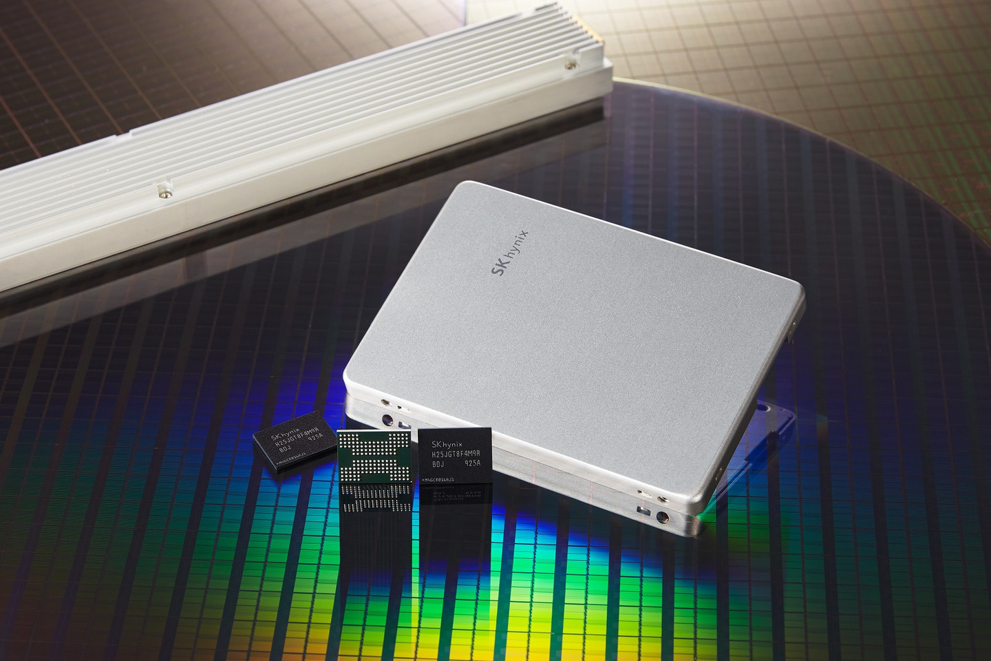
SK hynix Inc. announced today that it has developed and started mass-producing the world's first 128-Layer 1 Tb (Terabit) TLC (Triple-Level Cell) 4D NAND Flash, only eight months after the Company announced the 96-Layer 4D NAND Flash last year.
The 128-Layer 1 Tb NAND chip offers the industry's highest vertical stacking with more than 360 billion NAND cells, each of which stores 3 bits, per one chip. To achieve this, SK hynix applied innovative technologies, such as "ultra-homogeneous vertical etching technology," "high-reliability multi-layer thin-film cell formation technology," and ultra-fast low-power circuit design, to its own 4D NAND technology.
The new product provides the industry's highest density of 1 Tb for TLC NAND Flash. A number of companies including SK hynix have developed 1 Tb QLC (Quad-Level Cell) NAND products, but SK hynix is the first to commercialize the 1 Tb TLC NAND Flash. TLC accounts for more than 85% of the NAND Flash market with excellent performance and reliability.
 The small chip size, the biggest advantage of the Company's 4D NAND, allowed SK hynix to realize ultra-high-density NAND Flash memory. The Company announced the innovative 4D NAND in October 2018, which combined 3D CTF (Charge Trap Flash) design with the PUC (Peri. Under Cell) technology.
With the same 4D platform and process optimization, SK hynix was able to reduce the total number of manufacturing processes by 5% while stacking 32 more layers on the existing 96-Layer NAND. As a result, the investment cost for the transition from 96-Layer to 128-Layer NAND has been reduced by 60% compared to the previous technology migration, significantly boosting investment efficiency.
The 128-Layer 1 Tb 4D NAND increases bit productivity per wafer by 40% compared to the Company's 96-Layer 4D NAND.
SK Hynix will start shipping the 128-Layer 4D NAND flash from the second half of this year, while continuing to roll out various solutions.
With its four-Plane architecture in a single chip, this product achieved a data transfer rate of 1,400 Mbps (Megabits/sec) at 1.2 V, enabling high-performance and low-power mobile solutions and enterprise SSD.
SK Hynix plans to develop the next-generation UFS 3.1 product in the first half of next year for major flagship smartphone customers. With 128-Layer 1 Tb NAND Flash, the number of NAND chips necessary for a 1 TB (Terabyte) product, currently the largest capacity for a smart phone, will be reduced by half, compared to 512 Gb NAND; it will provide customers with a mobile solution with 20% less power consumption in a 1 mm-thin package.
The Company also intends to start mass production of a 2 TB client SSD with an in-house controller and software in the first half of next year. 16 TB and 32 TB Non-Volatile Memory express (NVMe) SSDs for cloud data centers will be released next year as well.
"SK Hynix has secured the fundamental competitiveness of its NAND business with this 128-Layer 4D NAND," said Executive Vice President Jong Hoon Oh, Head of Global Sales & Marketing. "With this product, with the industry's best stacking and density, we will provide customers with a variety of solutions at the right time."
SK Hynix is developing the next-generation 176-Layer 4D NAND Flash, and will continue to strengthen the competitiveness of its NAND business through technological advantages.
The 128-Layer 1 Tb NAND chip offers the industry's highest vertical stacking with more than 360 billion NAND cells, each of which stores 3 bits, per one chip. To achieve this, SK hynix applied innovative technologies, such as "ultra-homogeneous vertical etching technology," "high-reliability multi-layer thin-film cell formation technology," and ultra-fast low-power circuit design, to its own 4D NAND technology.
The new product provides the industry's highest density of 1 Tb for TLC NAND Flash. A number of companies including SK hynix have developed 1 Tb QLC (Quad-Level Cell) NAND products, but SK hynix is the first to commercialize the 1 Tb TLC NAND Flash. TLC accounts for more than 85% of the NAND Flash market with excellent performance and reliability.

With the same 4D platform and process optimization, SK hynix was able to reduce the total number of manufacturing processes by 5% while stacking 32 more layers on the existing 96-Layer NAND. As a result, the investment cost for the transition from 96-Layer to 128-Layer NAND has been reduced by 60% compared to the previous technology migration, significantly boosting investment efficiency.
The 128-Layer 1 Tb 4D NAND increases bit productivity per wafer by 40% compared to the Company's 96-Layer 4D NAND.
SK Hynix will start shipping the 128-Layer 4D NAND flash from the second half of this year, while continuing to roll out various solutions.
With its four-Plane architecture in a single chip, this product achieved a data transfer rate of 1,400 Mbps (Megabits/sec) at 1.2 V, enabling high-performance and low-power mobile solutions and enterprise SSD.
SK Hynix plans to develop the next-generation UFS 3.1 product in the first half of next year for major flagship smartphone customers. With 128-Layer 1 Tb NAND Flash, the number of NAND chips necessary for a 1 TB (Terabyte) product, currently the largest capacity for a smart phone, will be reduced by half, compared to 512 Gb NAND; it will provide customers with a mobile solution with 20% less power consumption in a 1 mm-thin package.
The Company also intends to start mass production of a 2 TB client SSD with an in-house controller and software in the first half of next year. 16 TB and 32 TB Non-Volatile Memory express (NVMe) SSDs for cloud data centers will be released next year as well.
"SK Hynix has secured the fundamental competitiveness of its NAND business with this 128-Layer 4D NAND," said Executive Vice President Jong Hoon Oh, Head of Global Sales & Marketing. "With this product, with the industry's best stacking and density, we will provide customers with a variety of solutions at the right time."
SK Hynix is developing the next-generation 176-Layer 4D NAND Flash, and will continue to strengthen the competitiveness of its NAND business through technological advantages.

7 Comments on SK Hynix Starts Mass-Producing World's First 128-Layer 4D NAND, Working on 176-Layer NAND
I assume four-plane is reference to 4d nand.