Monday, October 5th 2020

AMD "Big Navi" GPU Die Pictured? Allegedly Measures 536mm²

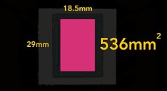
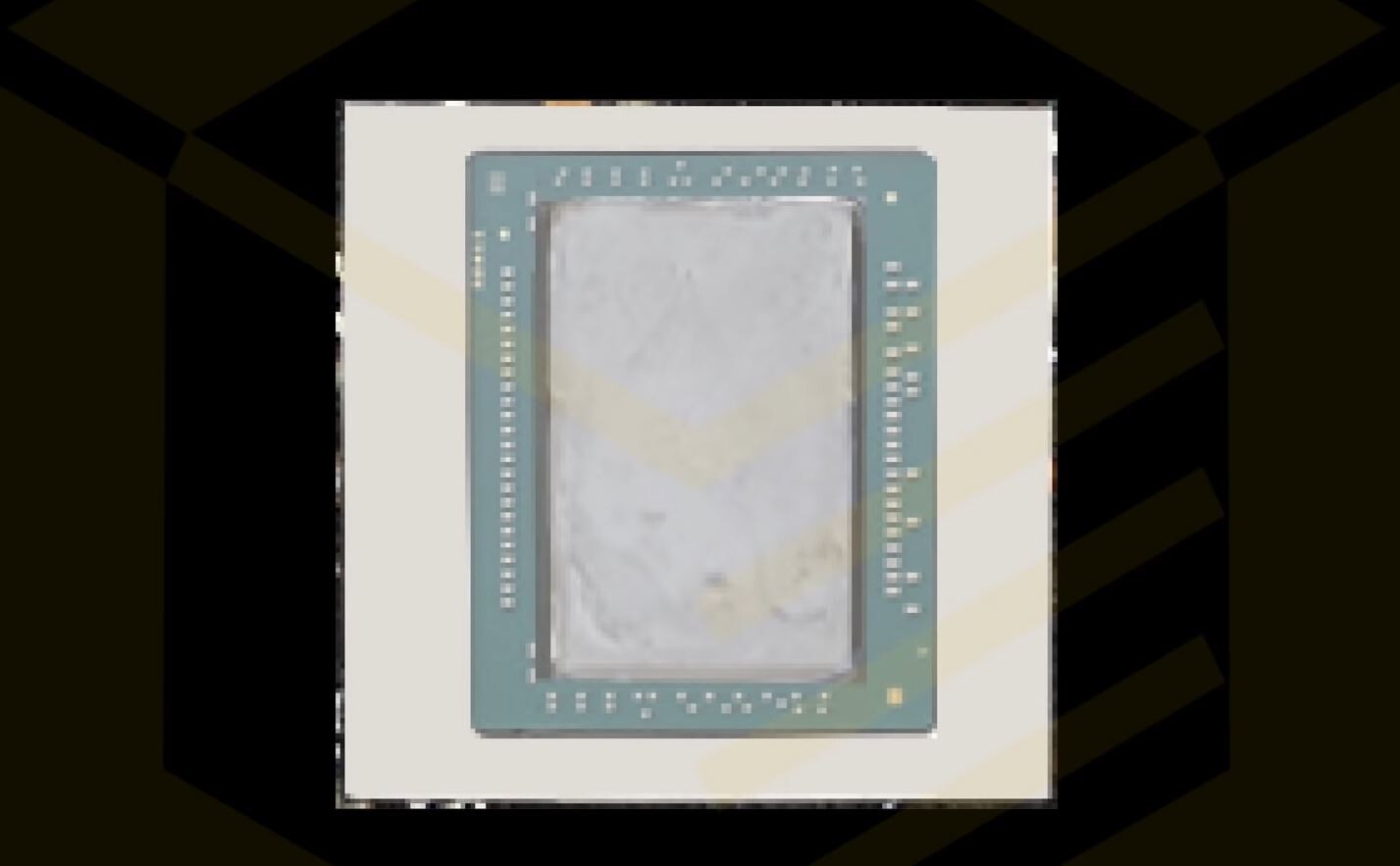
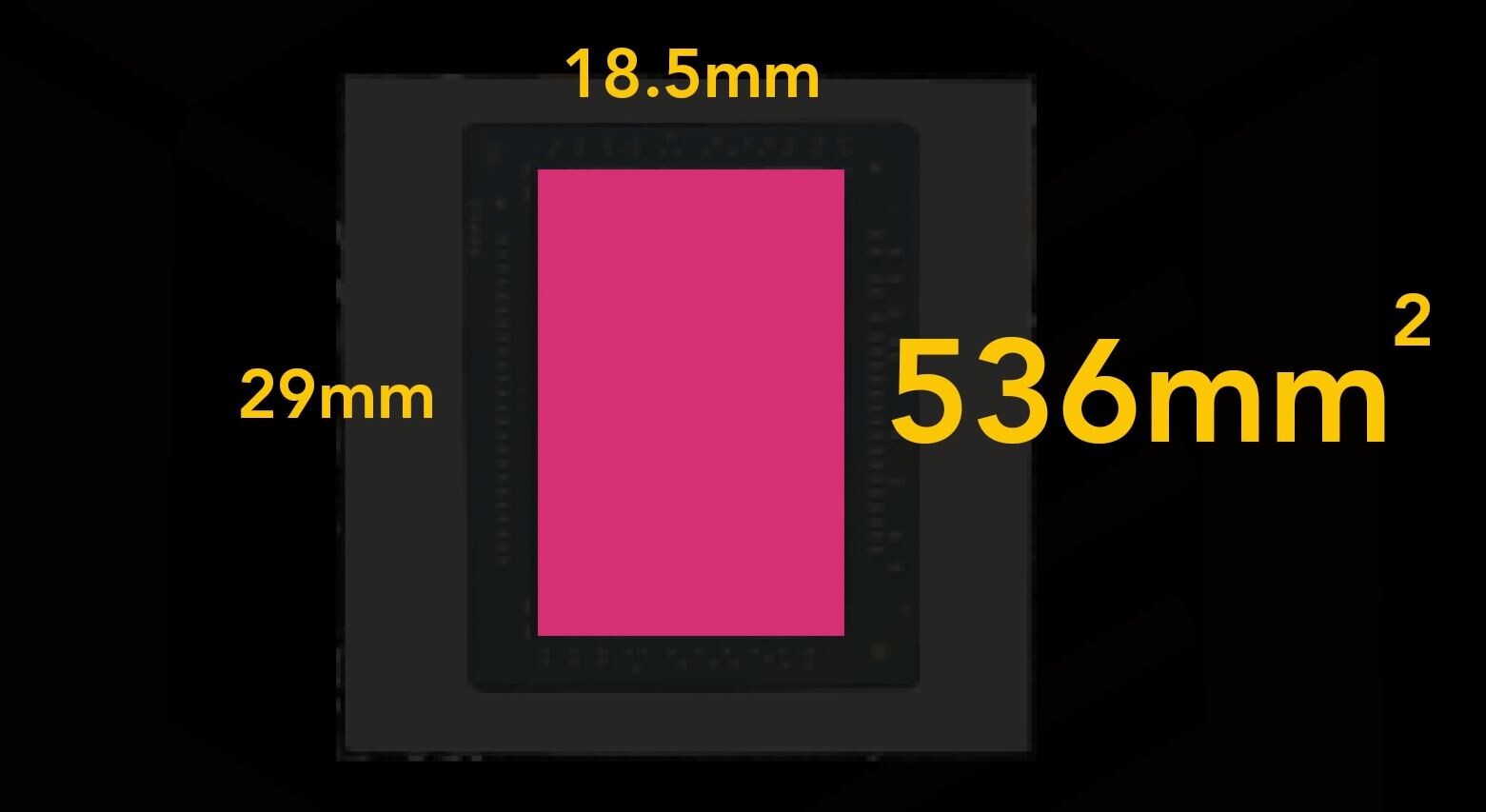
Coreteks, in a video presentation on Sunday, released what is possibly the very first picture of the AMD "Big Navi" GPU silicon, which could power the company's next-generation Radeon RX 6000 series flagship graphics card. The grainy, blurry-cam picture reveals a mostly square package with a large, rectangular die at its center, which Coreteks estimates to be 536 mm² in die-area, with 29 mm x 18.5 mm (LxW) dimensions. The channel used an unusual method for measuring the die size. The chip is rumored to feature around 80 compute units based on the RDNA2 graphics architecture, which includes fixed-function hardware for real-time raytracing, as RDNA2 is designed to meet DirectX 12 Ultimate logo requirements. We'll know more about the chip in the run up to its October 28 unveiling.
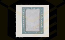
Source: Coreteks (YouTube)
Add your own comment

37 Comments on AMD "Big Navi" GPU Die Pictured? Allegedly Measures 536mm²

#26
Th3pwn3r
Jism5700 was a engineering wonder
Lol, good one.
Posted on Reply
#27
ValenOne
InVasManiAlso this no reasons...just felt it needed to be inserted into the matter. I wonder if anyone's ever been crazy enough to get that as a tattoo.
For GA102 vs TU102, Nvidia doubles the CUDA core count with a minor increase in GPC (incudes a rasterzation unit) count. Your argument is hypocritical.
Posted on Reply
#28
AnarchoPrimitiv
Th3pwn3rLol, good one.
What's not impressive about a company with a third of the budget able to compete? I think that's really impressive
Posted on Reply
#29
Th3pwn3r
AnarchoPrimitivWhat's not impressive about a company with a third of the budget able to compete? I think that's really impressive
You act as if both companies are one trick ponies. They don't just allocate all of their resources into one thing. And as more of a high end user I'm not impressed when someone's best is another's mid grade.
Posted on Reply
#30
ARF
Jism5700 was a engineering wonder, pretty much the staff being challenged to make a base chip, medium GPU size and still compete with Nvidia's offerings.
It competes with Nvidia's medium sized GPUs. Which have all the CUDA and RT hardware and still have the same number of transistors.

5700 is a shrink, try to make it on 16nm.
Posted on Reply
#31
TheoneandonlyMrK
ARFIt competes with Nvidia's medium sized GPUs. Which have all the CUDA and RT hardware and still have the same number of transistors.

5700 is a shrink, try to make it on 16nm.
Wrong, you don't shrink an old architecture and miraculously create a new architecture.

Who the f knows what it competes with, if you have FACT based proof rather than the wafts of air an ass puts out, please ,do show.
Posted on Reply
#32
Punkenjoy
Big If there,

but if the infinity cache help to alleviate the performance drawback of a "Only" 256 bit bus for big Navi. this will do incredibly well with Integrated GPU that are even more bandwidth starved. if it's that, this litteraly mean a Jump in integrated GPU performance.

It could also explain why they did more of Vega APU while they were focusing on getting RDNA2 done.
Posted on Reply
#33
ARF
theoneandonlymrkthe wafts of air an ass puts out
If the moderators don't use double standards, they have to address this personal attack and trolling.
Posted on Reply
#34
evernessince
PunkenjoyBig If there,

but if the infinity cache help to alleviate the performance drawback of a "Only" 256 bit bus for big Navi. this will do incredibly well with Integrated GPU that are even more bandwidth starved. if it's that, this litteraly mean a Jump in integrated GPU performance.

It could also explain why they did more of Vega APU while they were focusing on getting RDNA2 done.
The more exciting part is the potential for performance improvements it could bring. Yes it could help memory bandwidth but having what is essentially a large L3 cache on the GPU could drastically speed up games. Imagine frequently accessed game engine data that was previously being stored on the VRAM is instead on the infinity cache. You are talking about a massive improvement to latency and bandwidth.
Posted on Reply
#35
bug
That die size puts an upper limit on expectations: double the size means double the transistor count (they're both 7FF). Subtract the area for RTRT (Turing used like 20% die area), the rumored increase in cache sizes and you get 75% more CUs, tops. If AMD can put all that to good use, they may be on to something. The downside, as Turing reminded us, is dies that big don't come cheap.
Posted on Reply
#36
InVasMani
evernessinceThe more exciting part is the potential for performance improvements it could bring. Yes it could help memory bandwidth but having what is essentially a large L3 cache on the GPU could drastically speed up games. Imagine frequently accessed game engine data that was previously being stored on the VRAM is instead on the infinity cache. You are talking about a massive improvement to latency and bandwidth.
We already saw a bit of this with Intel's desktop Broadwell with the EDRAM, but this appears a bit more advanced. Regardless if true I can defiantly see it hopefully providing a nice impact to 1% and 0.1% percentiles that are latency sensitive. Some of that of course depends on how much can fit into the cache and how it gets allocated.
Posted on Reply
Add your own comment
Apr 18th, 2024 09:03 EDT change timezone

New Forum Posts

Popular Reviews

Controversial News Posts