Wednesday, June 30th 2021

Samsung 3 nm GAAFET Node Delayed to 2024
Samsung's ambitious 3 nm silicon fabrication node that leverages the Gate All Around FET transistors, has reportedly been delayed to 2024. The company brands this specific node as 3GAE. 2024 is the earliest date when Samsung will be able to mass-produce chips on 3GAE, which means the company, along with Intel, will begin to fall significantly behind TSMC on foundry technology. The Taiwanese semiconductor fabrication giant will target 2 nm-class nodes around 2024, which leverages EUV multi-patterning, extensive use of cobalt in contacts and interconnects, germanium doped channels, and other in-house innovations. With Intel's foundry technology development slowing to a crawl in the sub-10 nm domain, Samsung is the only viable alternative to TSMC for cutting-edge logic chip manufacturing.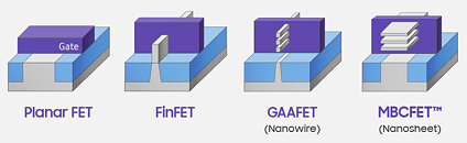
Source:
SemiAnalysis

11 Comments on Samsung 3 nm GAAFET Node Delayed to 2024
thats scary tbh.
TMSC's in-house innovation at work there ^^^^
It looks like I'm missing part of the picture. What happened with Global Foundries?
It’s clear that shrinking transistors and getting commercially viable yields is incredibly difficult… hence chiplets and tiles. Kudos to TSMC for its continued cadence.
Right now, Qualcomm is using them for the disappointing 888, but a delay this bad will almost certainty cost them the successor.
I(f both Qualcomm and Apple won't use you, then you have none of the early high-margin process node subsidizers (which means you will have less margin for next-gen R&D).
Samsung is a lot bigger than GF, but if they never make-up the 4- year deficit , it will eventually bleed them dry!
semiwiki.com/semiconductor-manufacturers/intel/295767-intel-nodes/
This wasn't really relevant because only Intel used Intel fabs too, so Samsung was the only competitor to TSMC after Global Foundries dropped out.
Hopefully Intel manages to not delay their 7nm anymore, which as far as report and rumor's goes rn, it's not looking that bad. And if they also succeed with their new foundry division, I think it would be some pretty good competition with TSMC.