Monday, October 2nd 2023

More AMD "Strix Point" Mobile Processor Details Emerge
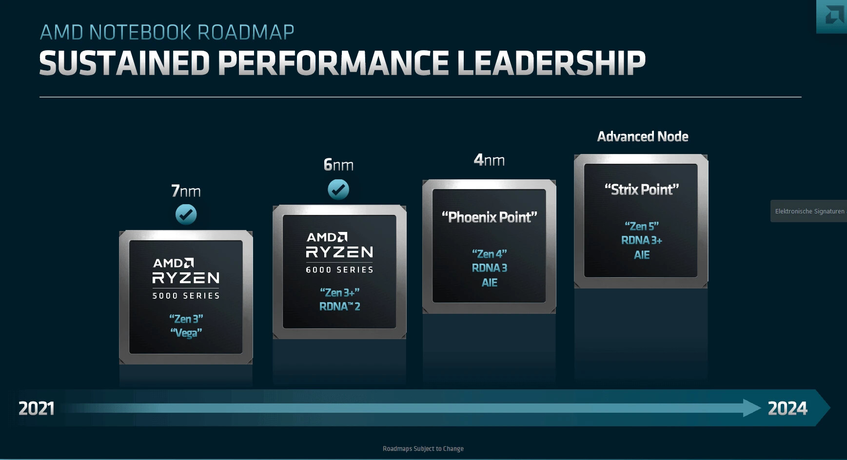
"Strix Point" is the codename for AMD's next-generation mobile processor succeeding the current Ryzen 7040 series "Phoenix." More details of the processor emerged thanks to "All The Watts!!" on Twitter. The CPU of "Strix Point" will be heterogenous, in that it will feature two different kinds of CPU cores, but with essentially the same ISA and IPC. It is rumored that the processor will feature 4 "Zen 5" CPU cores, and 8 "Zen 5c" cores.
Both core types feature an identical IPC, but the "Zen 5" cores can hold onto higher boost frequencies, and have a wider frequency band, than the "Zen 5c" cores. From what we can deduce from the current "Zen 4c" cores, "Zen 5c" cores aren't strictly "efficiency" cores, as they still offer the full breadth of core ISA as "Zen 5," including SMT. In its maximum configuration, "Strix Point" will hence be a 12-core/24-thread processor. The two CPU core types sit in two different CCX (CPU core complexes), the "Zen 5" CCX has 4 cores sharing a 16 MB L3 cache, while the "Zen 5c" CCX shares a 16 MB L3 cache among 8 cores. AMD will probably use a software-based solution to ensure the right kind of workload from the OS is processed by the right kind of CPU core. As for the integrated graphics, AMD is expected to deploy a large new iGPU based on the more advanced RDNA 3.5 graphics architecture, which has been referenced as "RDNA3+." It features 8 WGPs, or 16 CU, amounting to 1,024 stream processors, 64 TMUs, and an unknown number of ROPs (possibly 32), with the probable design goal of offering graphics performance close to a discrete Radeon RX 6500 XT graphics card. AMD will debut its second generation of the XDNA accelerator, the hardware backend of Ryzen AI. On "Strix Point," the accelerator is rumored to feature 64 AI Engines.
The chip's I/O is expected to be largely similar, with increase DDR5 memory speeds on offer—dual-channel (4x sub-channel) DDR5-5600 or LPDDR5X-8533, we don't know if AMD will update the PCIe interface to Gen 5 spec, the current "Phoenix" silicon is limited to Gen 4.
At this point, we don't know if "Strix Point" is a monolithic silicon, or a tiled processor, but AMD is expected to leverage the TSMC N4E (second gen 4 nm EUV) foundry node, for at least one of the tiles, or the whole die, in case this is a monolithic chip, with a total chip-area of around 225 mm².
Sources:
All The Watts!! (Twitter), Hardware Times
Both core types feature an identical IPC, but the "Zen 5" cores can hold onto higher boost frequencies, and have a wider frequency band, than the "Zen 5c" cores. From what we can deduce from the current "Zen 4c" cores, "Zen 5c" cores aren't strictly "efficiency" cores, as they still offer the full breadth of core ISA as "Zen 5," including SMT. In its maximum configuration, "Strix Point" will hence be a 12-core/24-thread processor. The two CPU core types sit in two different CCX (CPU core complexes), the "Zen 5" CCX has 4 cores sharing a 16 MB L3 cache, while the "Zen 5c" CCX shares a 16 MB L3 cache among 8 cores. AMD will probably use a software-based solution to ensure the right kind of workload from the OS is processed by the right kind of CPU core.
The chip's I/O is expected to be largely similar, with increase DDR5 memory speeds on offer—dual-channel (4x sub-channel) DDR5-5600 or LPDDR5X-8533, we don't know if AMD will update the PCIe interface to Gen 5 spec, the current "Phoenix" silicon is limited to Gen 4.
At this point, we don't know if "Strix Point" is a monolithic silicon, or a tiled processor, but AMD is expected to leverage the TSMC N4E (second gen 4 nm EUV) foundry node, for at least one of the tiles, or the whole die, in case this is a monolithic chip, with a total chip-area of around 225 mm².
16 Comments on More AMD "Strix Point" Mobile Processor Details Emerge
For an area equivalent to eight P cores, Intel's design, in which two of the P cores are replaced by E cores, has an MT performance equivalent to ten P cores. Strix Point, on the other hand, seems to have chosen to allocate four of the area of eight full cores to a reduced core to obtain MT performance equivalent to 12 cores.
The Phoenix Point is about 180mm², which is too much area for the V-Cache. To make mobile V-Cache, we need to do something we don't do now, such as removing all L3 from the main die and using a dedicated cache die for all L3 or L2. I don't think we will do all-V-Cache because it would mean abandoning everything except games.
www.anandtech.com/show/20010/the-asus-rog-strix-scar-17-2023-laptop-review-ryzen-9-7945hx3d-with-3d-v-cache-impresses
www.notebookcheck.net/Asus-ROG-Strix-SCAR-17-X3D-review-The-world-s-fastest-gaming-laptop.742941.0.html
As for the physical implementation itself pretty sure AMD has probably half a dozen ways to skin the cat.
C and non-C cores will be part of the same CCX. To do anything else with the available time-to-design and TSMC capabilities would place AMD further behind Intel for chips of this type.
AMD and partners would also be dealing with uneven distribution of heat across the package with c on one half and non-c on the other. That certaintly wouldnt work for desktop solutions.
I'll sit back and let this this post age like fine whine and you can see for yourself.
Of course AMD may also do something unexpected again with Zen 5, like packing 5c cores in clusters of two or four, and then the perf-power-area balance becomes less predictable.
I am also intrigued by the possibility (to clarify, this is something that I thought of; there is no reason to believe that AMD is planning on doing this) of having Zen C X3D CCDs, as the lower power, and thus heat output, of Zen C combined with the reduced L2 cache might pair nicely with 3D V-Cache.
Gracemont vs Golden Cove
both at the same 2.0 GHz
MT perf./power: 1.0x
MT perf./area: 1.6x
ST perf.: 0.65x
both at their own maximum clock (3.8 GHz vs 5.2 GHz)
MT perf./power: 1.5x
MT perf./area: 1.2x
ST perf: 0.5x
Zen 4c vs Zen4
both at the same 2.0 GHz
MT perf./power: 1.0x
MT perf./area: 1.54x
ST perf.: 1.0x
both at own maximum clock (3.5 GHz vs 4.8 GHz)
MT perf./power: 1.0x
MT perf./area: 0.95x
ST perf: 0.75x