Friday, December 12th 2025

Apple A19 Pro & A19 Die Size Analysis Indicates 9-10% Smaller Than A18 Models
Apple launched its A19 Pro and A19 mobile processors about three months ago. The 3 nm 64-bit Arm-based SoCs drive a new wave of iPhone 17 series smartphones, as well as the ultraslim + lightweight iPhone Air. It took a while for close-up die shots to emerge from independent groups. Eventually, close-ups of the A19 Pro's layout turned up online, mid-way through November. Investigations have focused on Apple's selection of TSMC's cutting-edge N3P node process; granting a noticeable reduction in die areas, when compared to previous-gen equivalents. 2024's A18 Pro and A18 designs are 3 nm chips, but manufactured via N3E (FinFET)—an older/less advanced node. The leading foundry's N3P product is referred to as a "high-performance variant."
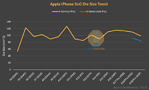
When comparing the current flagship chipset (A19 Pro) to its predecessor (A18 Pro), keen observers noted a 10% reduction in footprint—going from 105 mm² down to 98.6 mm². Additionally, SemiAnalysis reckons that the A19 is 9% smaller than its forebear (A18). According to their calculations, the upgrade to N3P would only grant about a 4% difference in area. Logically, Apple's engineering team must have played around with other aspects in order to reach nine to ten percent shrinkage. SemiAnalysis outlined important improvements across the latest chip designs: "looking at core areas, The P-Core shrank by 4%, while the E-Core and GPU are 10% larger, reflecting the increased transistor budget for the large efficiency gains seen in benchmarks...The cache macro doubled in size to 32 KB for a 10% higher density cache: A18 4 MB of SLC: 1.08 mm², and A19 4 MB of SLC: 0.98 mm². There's also a more area efficient layout of all the minor 'uncore' SOC area (e.g. display/media engine, ISP, security etc)." In conclusion, they propose that several smart design innovations have lead to "an area reduction comparable to a major node shrink," overall a big achievement, albeit in a smaller package.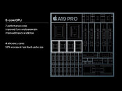


Sources:
SemiAnalysis Tweet, Kurnal Tweet (die Shot - historical), Wccftech, Notebookcheck, Cardyak Tweet (die shot), Tieba Baidu
When comparing the current flagship chipset (A19 Pro) to its predecessor (A18 Pro), keen observers noted a 10% reduction in footprint—going from 105 mm² down to 98.6 mm². Additionally, SemiAnalysis reckons that the A19 is 9% smaller than its forebear (A18). According to their calculations, the upgrade to N3P would only grant about a 4% difference in area. Logically, Apple's engineering team must have played around with other aspects in order to reach nine to ten percent shrinkage. SemiAnalysis outlined important improvements across the latest chip designs: "looking at core areas, The P-Core shrank by 4%, while the E-Core and GPU are 10% larger, reflecting the increased transistor budget for the large efficiency gains seen in benchmarks...The cache macro doubled in size to 32 KB for a 10% higher density cache: A18 4 MB of SLC: 1.08 mm², and A19 4 MB of SLC: 0.98 mm². There's also a more area efficient layout of all the minor 'uncore' SOC area (e.g. display/media engine, ISP, security etc)." In conclusion, they propose that several smart design innovations have lead to "an area reduction comparable to a major node shrink," overall a big achievement, albeit in a smaller package.


5 Comments on Apple A19 Pro & A19 Die Size Analysis Indicates 9-10% Smaller Than A18 Models
Must be the fruity bois new M.O. Or perhaps just a refinement of their existing processes.
Now if they can do this in order to keep iPhone prices down while increasing performance (which appears to be their goal), then mo powah to them :D
P-Core L2 Cache: 16MB (shared)
P-Core L1 Cache: ?kB (per core)
E-Core L2 Cache: 6MB (shared)
E-Core L1 Cache: ?kB (per core)
SoC LLC Cache: 32MB (shared)
NPU Cache: 2MB (shared)
NPU Cache: 128kB (per core)
...
Every cache is build with a number of individual cache-blocks. Apple seems to have tweaks the way the overall assembly and each block itself, which results in the 10% area gain. It quite noticable to get these gains in minor node improvements, especially since cache cells usually don't shrink as much as logic cells.