Friday, January 30th 2026

AMD "Zen 6" CCD Packs 12 Cores, 48 MB L3 Cache
The standard CPU complex die (CCD) chiplet based on AMD's next-generation "Zen 6" microarchitecture is poised to feature a 50% increase in CPU core counts. This would be the first time that AMD has increased core-counts of its CCDs containing full-sized CPU cores capable of sustaining high clock speeds. It had developed CCDs with high core counts using compacted cores with lower clock speed limits until now. The standard "Zen 6" CCD is expected to come with a similar die-size to the current "Zen 5" CCD, with a rumored die size of 76 mm², which is slightly larger than the 71 mm² of the "Zen 5" CCD.
The "Zen 6" CCD is expected to pack 12 CPU cores, all part of a single CPU core complex (CCX). All twelve cores share a 48 MB L3 cache. Both the CPU core counts and L3 cache size hence see a 50% increase over "Zen 5." AMD is building the "Zen 6" CCD on TSMC N2 (2 nm nanosheet) process node, which evidently offers a massive increase in transistor densities over the current TSMC N4P (4 nm FinFET) on which the "Zen 5" CCD is made. With an eye on Intel's pivot towards a cache rebalancing in favor of large last-level caches on some of its premium Core Ultra 400 "Nova Lake-S" desktop processors, AMD is expected to give the "Zen 6" CCD full 3D V-Cache capability, and the company's next X3D processors could come with L3 caches of 144 MB per CCD for up to 288 MB of L3 cache on the desktop AM5 socket.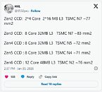
Sources:
HXL (Twitter), VideoCardz
The "Zen 6" CCD is expected to pack 12 CPU cores, all part of a single CPU core complex (CCX). All twelve cores share a 48 MB L3 cache. Both the CPU core counts and L3 cache size hence see a 50% increase over "Zen 5." AMD is building the "Zen 6" CCD on TSMC N2 (2 nm nanosheet) process node, which evidently offers a massive increase in transistor densities over the current TSMC N4P (4 nm FinFET) on which the "Zen 5" CCD is made. With an eye on Intel's pivot towards a cache rebalancing in favor of large last-level caches on some of its premium Core Ultra 400 "Nova Lake-S" desktop processors, AMD is expected to give the "Zen 6" CCD full 3D V-Cache capability, and the company's next X3D processors could come with L3 caches of 144 MB per CCD for up to 288 MB of L3 cache on the desktop AM5 socket.

99 Comments on AMD "Zen 6" CCD Packs 12 Cores, 48 MB L3 Cache
upload.wikimedia.org/wikipedia/commons/2/2d/Socket_AM5_pinmap.svgWith some flexibility in using the lanes the amount of them would not be so restrictive.
But really, what would alleviate Zen 4/5/6's lane shortage would be if AMD would just allow board manufacturers to allocate and bifurcate those lanes. So for example, Instead of forcing x16 GPU (slot) + x4 SSD +x4 SSD, a manufacturer should be able to offer a board with triple slots that each run at x8.
Intel and AMD build their consumer platform with consumer in mind, not professional. They have professional platform that will provide what you needs. Some might think they need professional platforms for their daily usage, but they just have to buy the professional platform.
It always have been like that
The reason you don't see three x8 much is cost / benefit. The vast majority of people just stick a GPU in there and are done slot wise. Both PCIe 4.0 and 5.0 require a repeater and 5.0 requires more layers as well. The requirements will get even worse with PCIe 6.0.
As for the discussion of what people need, pure gamers can do fine on AM5, but they better choose one of the few motherboards which allows those 4 lanes reserved for USB 4 to be used for an additional M.2 or PCIe slot, as otherwise they will be left with only one SSD at full speed and one (or more) sharing bandwidth through the chipset. Pretty much any power user would at least want 3 "full speed" SSDs; OS, games and work drive, and on AM5 one of those will in practice have to run at "half speed". With higher tier boards coming for the next gen we can expect motherboards to feature 10G NICs, which alone will suck up 1 lane from the chipset, which further emphasizes the need for bandwidth.
And while splitting the x16 slot is fine for some, we are talking about prosumers here, and assuming someone would want to upgrade the GPU one or two generations from now when GPUs will be PCIE 6.0, having those x16 lanes for the GPU alone will become important.
the am5 chipset / hub sharing is a cost feature and on purpose. i do not expect that to be solved.
it is nice to not see pcie 3 ssds anymore on am5. the main reason for my am5 transition. 1x pcie 3x4 amd 1x pcie 4.0 was too slow. multiple pcie 4.0x4 are fine.
why else would someone not buy threadripper?
Throw off that crappy Prom21 and you can get that. Three x8 at Gen5 speed.
+ 1x 480 Mbps USB 2.0
+ 4x 10 Gbps USB 3.2 Gen 2
- no SATA- no NVME
Edit: 28 lanes total = 3 groups of x8 + one x4 to chiplet
Sorry. Was confused by TPU database showing 24 lanes. Its 24 usable lanes after connecting chiplet.There is a "little" issue. Prom21 uses 4 lanes. But work only at Gen4 speed (half of bandwidth that Ryzen 7000/9000 provides).On the motherboards already providing Gen5 PCIe lanes to GPU, NVME, USB4 it would not increase cost (so much) for another 4 lanes to chipset. Even if chipset itself would provide only Gen4 lanes.
But you have to ask AsMedia when they will condescend to learn how to use Gen5 in their chips.Older ones (600 series) where USB4 was not mandatory.
Or some of the few 800 series which allow user to chose where they want use those Gen5 lanes.Without sacrificing lanes from GPU:
AM5 - 2 NVME slots Gen5 x4
s1700 - zero
s1851 - 2 NVME slots Gen5 x4
Any more and you use lanes from GPU or "half-speed" lanes from chipset.With enough of VRAM at GPU the difference between PCIe Gen speed is marginal.
All of those miners used GPU connected via x1 Gen3.
Yes, I referenced gaming performance on a high core count part. It's not that think having 12 or 24 cores is going to make a huge difference in most games, I just want high core counts for other applications without having to take a hit to gaming performance.
The 52 core will consume ~400W and be threadwripper priced (doubling core count and going from 3->2nm when your best chip consumes 253W under multithread, 379.5 and thats expecting them to NOT raise clocks and have perfect scaling).