Wednesday, February 4th 2026

AMD Announces Kintex UltraScale+ Gen 2 FPGAs to Capture the Middle of the Market
AMD today unveiled the Kintex UltraScale+ Gen 2 FPGA family. The company's latest announcement is a strategic play for the middle-of-the-market in the FPGA segment that's dominated by the likes of Intel Agilex 5 series. Targeting sectors that demand longevity and reliability, such as medical imaging, industrial automation, and broadcast video production, the Gen 2 family is not just a lithography shrink, but it represents a significant architectural modernization of the existing 16 nm Kintex platform, infusing it with the high-speed connectivity and memory standards required for the data-heavy workloads of 2027 and beyond.
The original Kintex UltraScale+ series from the Xilinx era is popular in the industry, for a performance/Watt balance that made it the suitable for everything from ultrasound machines to 5G radio heads. However, as edge devices have become hungrier for bandwidth, the original platform's connectivity options began to show their age. The Gen 2 update addresses the I/O modernization need. The most striking upgrade is the memory subsystem, replacing DDR4 with newer LPDDR4X, DDR5 and LPDDR5X memory standards. LPDDR tends to be popular for compact, edge devices in the IIoT (industrial IoT) space. This should even pave the way for a new crop of 8K or 4K broadcast-tier cameras. Since these are produced in small batches, FPGAs are preferred over ASICs or elaborate SoCs.
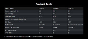 Memory is a key part of the I/O AMD updated with Kintex UltraScale+, the company also improved the chip's serial interconnects. To begin with, AMD is implementing PCI-Express Gen 4, an important update from the previous-gen chips that were limited to Gen 3, which should improve storage subsystem performance. The company also added dual 100G Ethernet MAC blocks, which should prove crucial in IIoT applications that rely on real-time data aggregation.
AMD is competing not just with Agilex 5 series, but also Lattice Semiconductor's Avant series. Intel's chips are built on the Intel 7 foundry node, while Lattice uses the older TSMC 16 nm FinFET node. AMD, interestingly, is building the Kintex UltraScale+ Gen 2 family on the same exact 16 nm node that the first generation was built on. By sticking with 16 nm for Kintex Gen 2, AMD is betting that customers value platform stability, lower NRE (Non-Recurring Engineering) costs, and supply assurance over the marginal density gains of a newer node. AMD is offering higher performance, a newer I/O, and LUT6 logic compared to LUT4 by Lattice. It also offers a higher maximum frequency (Fmax).
Tech and I/O are one aspect of FPGAs, but security is quite a different thing. You program FPGAs with your IP, but what if someone decides to copy that IP from the FPGA? AMD has integrated CNSA 2.0-grade cryptography, bitstream encryption, and anti-cloning protections directly into the silicon. This allows for secure, authenticated operation in "zero-trust" environments.
AMD is committing to making the series available till 2045, which should make the product line particularly appealing to industries with extremely long product lifecycles, such as aerospace and defense. There are still airplanes in the sky that need navigation data fed to them using 5.25-inch floppy disks. That's how long product lifecycles can be in this segment.
AMD is planning to make Kintex UltraScale+ Gen 2 support available to Vivado and Vitis tools in Q3-2026. The first engineering samples of the chip should reach target audience by Q4-2026. Mass production of the chips should commence in the first half of 2027.
Source:
AMD
The original Kintex UltraScale+ series from the Xilinx era is popular in the industry, for a performance/Watt balance that made it the suitable for everything from ultrasound machines to 5G radio heads. However, as edge devices have become hungrier for bandwidth, the original platform's connectivity options began to show their age. The Gen 2 update addresses the I/O modernization need. The most striking upgrade is the memory subsystem, replacing DDR4 with newer LPDDR4X, DDR5 and LPDDR5X memory standards. LPDDR tends to be popular for compact, edge devices in the IIoT (industrial IoT) space. This should even pave the way for a new crop of 8K or 4K broadcast-tier cameras. Since these are produced in small batches, FPGAs are preferred over ASICs or elaborate SoCs.


AMD is competing not just with Agilex 5 series, but also Lattice Semiconductor's Avant series. Intel's chips are built on the Intel 7 foundry node, while Lattice uses the older TSMC 16 nm FinFET node. AMD, interestingly, is building the Kintex UltraScale+ Gen 2 family on the same exact 16 nm node that the first generation was built on. By sticking with 16 nm for Kintex Gen 2, AMD is betting that customers value platform stability, lower NRE (Non-Recurring Engineering) costs, and supply assurance over the marginal density gains of a newer node. AMD is offering higher performance, a newer I/O, and LUT6 logic compared to LUT4 by Lattice. It also offers a higher maximum frequency (Fmax).
Tech and I/O are one aspect of FPGAs, but security is quite a different thing. You program FPGAs with your IP, but what if someone decides to copy that IP from the FPGA? AMD has integrated CNSA 2.0-grade cryptography, bitstream encryption, and anti-cloning protections directly into the silicon. This allows for secure, authenticated operation in "zero-trust" environments.
AMD is committing to making the series available till 2045, which should make the product line particularly appealing to industries with extremely long product lifecycles, such as aerospace and defense. There are still airplanes in the sky that need navigation data fed to them using 5.25-inch floppy disks. That's how long product lifecycles can be in this segment.
AMD is planning to make Kintex UltraScale+ Gen 2 support available to Vivado and Vitis tools in Q3-2026. The first engineering samples of the chip should reach target audience by Q4-2026. Mass production of the chips should commence in the first half of 2027.
8 Comments on AMD Announces Kintex UltraScale+ Gen 2 FPGAs to Capture the Middle of the Market
:p
Even AMD's highest-end FPGA's only have a few hundred Megabits of RAM.
www.amd.com/en/products/adaptive-socs-and-fpgas/fpga/virtex-ultrascale-plus.html#product-table
(source - AMD)
From another point of view, even RAM and flash manufacturers always state the chip capacity in bits, not bytes.
It's all very fast static RAM blocks, similar to cache on CPU. It's also spread all over the chip because many IP blocks require a bit of RAM to work.
For anything else like big buffers, work space or embedded CPU RAM there are the external DRAM ports.
But that's all optional, in many applications you don't need external DRAM at all and that simplifies design and frees the pins for another use as I/Os.
It's specified in megabits because the word width is flexible, it can be arranged in many different ways as noted above, so bits make sense. 8 bit words are only one of many ways how to use it...