Wednesday, April 22nd 2026
Bolt Graphics Completes Tape-Out of Test Chip for Its Zeus GPU
Bolt Graphics today announced the successful tape-out of its test chip, marking a key milestone in the development of its Zeus GPU. Zeus is a next-generation compute platform designed to reduce the total cost of compute by up to 17 times across high-performance computing (HPC), rendering, and emerging compute-intensive applications.
Global demand for compute capacity continues to accelerate to support capabilities such as simulations, real-time graphics, and artificial intelligence across a wide range of industries. To address the need, companies optimized existing compute architectures for peak performance rather than cost efficiency, causing infrastructure cost to become a primary constraint. As the majority of workloads remain dependent on these architectures, large segments of the available market remain economically unviable.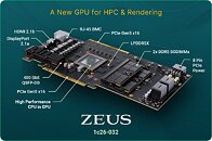
Bolt Graphics takes a fundamentally different approach to delivering compute to the market. The company achieves superior performance while optimizing for performance-per-dollar rather than maximizing for just peak performance. By focusing on cost efficiency at the system level, the Zeus platform delivers step-function improvements in compute economics. With cost savings up to 17 times compared to incumbent architectures, Zeus unlocks new classes of workloads previously constrained by cost.
The Zeus platform integrates a custom GPU architecture with a full software stack to create a unified system designed to operate across multiple compute markets. The platform uses established semiconductor processes, with the test chip successfully designed into TSMC 12 FFC. The Zeus scalable architecture also addresses advanced nodes, including 5 nm.
Initial offerings will target Zeus for HPC and rendering workloads. These workloads represent an addressable market exceeding $55 billion, where more than 90% of compute today still runs on CPUs. Bolt Graphics plans to expand into gaming and AI workloads as the platform scales.
Bolt Graphics expects Zeus to enter production in the fourth quarter of 2027.
Source:
Bolt Graphics
Global demand for compute capacity continues to accelerate to support capabilities such as simulations, real-time graphics, and artificial intelligence across a wide range of industries. To address the need, companies optimized existing compute architectures for peak performance rather than cost efficiency, causing infrastructure cost to become a primary constraint. As the majority of workloads remain dependent on these architectures, large segments of the available market remain economically unviable.

"Compute demand is growing exponentially, but cost remains the limiting factor," said Darwesh Singh, Founder and CEO/CTO of Bolt Graphics. "We believe the next generation of computing will be defined not just by performance but by efficiency. Our goal is to fundamentally change the economics of compute and become the default platform for next-generation workloads."Performance-Per-Dollar
Bolt Graphics takes a fundamentally different approach to delivering compute to the market. The company achieves superior performance while optimizing for performance-per-dollar rather than maximizing for just peak performance. By focusing on cost efficiency at the system level, the Zeus platform delivers step-function improvements in compute economics. With cost savings up to 17 times compared to incumbent architectures, Zeus unlocks new classes of workloads previously constrained by cost.
The Zeus platform integrates a custom GPU architecture with a full software stack to create a unified system designed to operate across multiple compute markets. The platform uses established semiconductor processes, with the test chip successfully designed into TSMC 12 FFC. The Zeus scalable architecture also addresses advanced nodes, including 5 nm.
"Moving from a rasterized pipeline in silicon to path tracing in silicon, at scale, is not an easy thing to do," said Dr. Ian Cutress, chief analyst, More Than Moore. "Bolt Graphics' Zeus test chip is an important first step toward cost-effective, fully accelerated path tracing for modern workloads, opening the door to a broader market and a new class of graphics acceleration beyond the limits of current graphics pipelines and products. This is a super exciting time for the industry, and I know a number of key industry players are keeping a close eye on Bolt's evolution."Bolt Graphics has already demonstrated strong early traction ahead of production, including a product pipeline exceeding $500 million, and over 14,000 members in their early access program, including enterprises, developers, and end users.
Initial offerings will target Zeus for HPC and rendering workloads. These workloads represent an addressable market exceeding $55 billion, where more than 90% of compute today still runs on CPUs. Bolt Graphics plans to expand into gaming and AI workloads as the platform scales.
Bolt Graphics expects Zeus to enter production in the fourth quarter of 2027.
8 Comments on Bolt Graphics Completes Tape-Out of Test Chip for Its Zeus GPU
That does take me back though.... Old ATi 3D Rage cards that would allow you to slot in extra ram. Some Matrox cards has this feature too. G200, Millennium.....
I can see the logic behind making an ASIC specifically for path-traced rendering workloads, which was their original pitch. Nvidia has to accommodate all types of workloads on their GPUs, so you could conceivably get better price/performance with a chip designed for a single workload. Of course it would still be an uphill battle against Nvidia's decades of experience and the pervasiveness of CUDA, but I could see it succeding if they got a major customer on board, like AWS and a Hollywood movie studio. You could even move into gaming after that.
But this? This is just competing directly against Vera Rubin and Bluefield. That's stupid.
Its simple.
Voilà ;)
But my guess is, that the company want's to get bought by nGreedia so they don't have to compete.