Wednesday, April 29th 2026

Intel Prepares HBM Killer: HB3DM Memory Stacks with Z-Angle Technology
Intel and SoftBank, through their subsidiary Saimemory, have been developing an alternative technology to the popular high-bandwidth memory (HBM) to provide more bandwidth and capacity for memory modules used with powerful AI accelerators. At VLSI 2026 in June, Saimemory is scheduled to present a paper on the newly developed HB3DM memory, which is based on Z-Angle Memory (ZAM) technology. This name refers to the vertical (Z-axis) stacking of dies, similar to traditional HBM. However, Intel aims to achieve impressive results using state-of-the-art manufacturing technology. The first generation of HB3DM will feature a total of nine layers, stacked using a hybrid bonding technique for 3D chip placement. At the base will be a logic layer that manages data movement within the chip, with eight DRAM layers on top for data storage. Each layer will include about 13,700 TSVs for hybrid bonding.
In terms of capacity, HB3DM will offer about 1.125 GB per layer, translating to 10 GB per memory module. Intel can achieve approximately 0.25 Tb/s of memory bandwidth per mm², and for a 10 GB module with a 171 mm² die area, we can expect around 5.3 TB/s per module. These impressive figures could quickly overshadow competing HBM4 memory, as HB3DM offers much higher bandwidth. HBM4 provides speeds of around 2 TB/s per stack, less than half of what HB3DM will deliver. However, HB3DM is limited by capacity, with only 10 GB available, whereas HBM4 can reach up to 48 GB per stack. Intel may increase the number of layers in production as HB3DM progresses, but for now, it is emerging as a bandwidth leader.
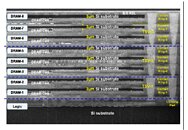
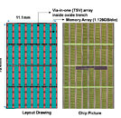
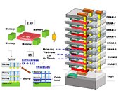 We don't yet know when Saimemory will launch these memory chips or who will manufacture the underlying DRAM. However, with Intel's involvement, there might be a return to DRAM manufacturing at Intel's fabs, although the specific node is currently unknown. As VLSI 2026 approaches, we expect to hear more details from both Intel and SoftBank about their Saimemory subsidiary and the progress they've made. Saimemory also plans to have prototypes ready by early 2028, with commercial products following in 2029.
Source:
via Ian Cutress on X
In terms of capacity, HB3DM will offer about 1.125 GB per layer, translating to 10 GB per memory module. Intel can achieve approximately 0.25 Tb/s of memory bandwidth per mm², and for a 10 GB module with a 171 mm² die area, we can expect around 5.3 TB/s per module. These impressive figures could quickly overshadow competing HBM4 memory, as HB3DM offers much higher bandwidth. HBM4 provides speeds of around 2 TB/s per stack, less than half of what HB3DM will deliver. However, HB3DM is limited by capacity, with only 10 GB available, whereas HBM4 can reach up to 48 GB per stack. Intel may increase the number of layers in production as HB3DM progresses, but for now, it is emerging as a bandwidth leader.


21 Comments on Intel Prepares HBM Killer: HB3DM Memory Stacks with Z-Angle Technology
I would love to see it on package for consumer soc's
That shortened path set should drop latency by a lot.
I mean this for regular consumers, not servers, since that is already available in form.
Also "for memory modules used with powerful AI accelerators"... Let's see if they move slow enough to entirely miss the AI craze. I mean it's Intel and SoftBank, if anyone can do it it's them.
PSMC?
Shinko Electric Industries?
Sandia national laboratories?
Lawrence Livermore national laboratory?
Los Alamos national laboratory?
NEDO?
RIKEN?
It’s hilarious when low information posters don’t bother doing the tiniest bit of research before expressing their opinion about technology that they have no awareness of.
UltraRAM Latest news
> Saimemory plans to have prototypes ready by early 2028, with commercial products following in 2029.
Name checks out though. Noise. Visible.
The above are all the organizations developing this memory. Sandia has already validated the design.
You do know what the Sandia National Laboratories is, right? On second thought I shouldn’t assume that either.
www.sandia.gov/research/news/from-early-rd-to-mature-technology/