Friday, July 17th 2026

Intel to Launch 28-Core "Nova Lake-S" Before 52-Core Version
Intel is gradually laying the groundwork for the launch of its Core Ultra 400 "Nova Lake-S" desktop processors with a basic branding overhaul. However, the company is reportedly preparing different launch dates for various SKUs, according to VideoCardz. We know that Intel has SKUs arriving with either one or two compute dies, featuring up to 8 "Coyote Cove" P-Cores and 16 "Arctic Wolf" E-Cores, along with 4 LPE-Cores that are part of the I/O die. Depending on the SKU, Intel can pack a single compute die for up to 28 cores total or two compute dies for a 52-core CPU SKU. It seems that the single compute die version will arrive first, with the dual compute die variants following. The 28-core "Nova Lake-S" DS version, a new SKU segment, is expected to launch in Q1 of 2027. For the regular overclocking-focused "K" SKUs, Intel reportedly plans an early Q2 launch between March and April.
What is particularly interesting to enthusiasts is when the 52-core compute powerhouse will launch. With its dual compute dies, Intel's most powerful desktop CPU is set to arrive between late May and September 2027, bringing this model to consumers. As for a possible reason why Intel is choosing such a schedule, we might assume that the recent change in plans to bring back most of the compute tile production on the 18A node is the reason. As Intel ramps up 18A high-volume manufacturing for its internal needs, the company likely needs more time to stockpile fully-fledged compute dies for the flagship 52-core SKUs. Since they require double the compute tiles compared to the 28-core designs, the production capacity may need to catch up first.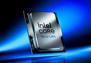
 Here is the roadmap plan, according to VideoCardz:
Source:
VideoCardz
What is particularly interesting to enthusiasts is when the 52-core compute powerhouse will launch. With its dual compute dies, Intel's most powerful desktop CPU is set to arrive between late May and September 2027, bringing this model to consumers. As for a possible reason why Intel is choosing such a schedule, we might assume that the recent change in plans to bring back most of the compute tile production on the 18A node is the reason. As Intel ramps up 18A high-volume manufacturing for its internal needs, the company likely needs more time to stockpile fully-fledged compute dies for the flagship 52-core SKUs. Since they require double the compute tiles compared to the 28-core designs, the production capacity may need to catch up first.


- NVL-S 28C DS: Q1 2027, late January to March 2027
- NVL-S 28C K: Q2 2027, March to April 2027
- NVL-S 16C and 8C: Q2 2027, late March to May 2027
- NVL-S 52C DS: Late May to September 2027
41 Comments on Intel to Launch 28-Core "Nova Lake-S" Before 52-Core Version
Intel has been far ahead of AMD in IPC on their P-cores for many years now, and that trend will only continue. Panther Cove-X will likely obliterate Zen 6 and even Zen 7 in IPC. The only reason there has been parity on desktop is because Intel uses E-cores as well. Which, while the E-cores have gotten pretty good, the overall per core performance is diminished because of them.
What people are wishing for is an end to artificial segmentation of markets, but ddr4 and 5 having the notch be different for rdimm vs ecc and electrically different enough makes that rather difficult.
for 2011v3 you could have an x99 board or a WS C612 board depending on the features you needed and not pay the workstation tax.
The explosion of core counts created such a large gap between server and consumer space that hedt got forgotten about and the workstation became a superclocked server variant.
LGA4677 and LGA4710-2 are sockets for workstations not HEDT, the distinction is the motherboard choices and purpose though intel is blurring the lines with overclocking support on workstation boards.
AMD skipped the HEDT variant of the threadripper for Zen3 and it greatly hurt that segment, but they got away with it because well... Intel hasn't been competing there.
I do also appreciate that AMD has just stuck to RDIMMS in the HEDT and WS threadrippers as unbuffered ecc has always cost more than rdimms and been capacity limited.
(David Huang, P-cores running at Fmax, AMD lead attributed to slightly higher boost clocks).
Unfortunately skatterbench uses different variants of cinebench in his GNR OC review vs the one he did for his Zen 4 TR one, but using his GB6 ST results, you see once again that RWC there has similar IPC as Zen 4 does.
This is LNC vs Zen 5 too, for reference:
Note that the 9900x and the 285K have similar boost clocks for their P-cores, so their scores here should be directly comparable for an IPC comparison. RPL (using GLC, which is very similar to RWC) seems like it comes close in total perf for specint2017, but that's due to the 7% bump in Fmax it has over the AMD part in this chart.
Here's another comparison from C&C between Zen 5 and RWC in GNR Xeon 6:
The AMD part has a ~24% higher score in specint2017 1T, however it also boosts ~13% higher than Intel's part, meaning that IPC should be ~ >10% higher (the greater than symbol because IPC decreases at higher clocks, hence why IPC comparisons are done best at iso frequency rather than dividing boost/perf at different boost clocks).
9965wx ... 350W / 24 cores = 14.58 W per core
9975wx ... 350W / 32 cores = 10.94 W per core
9985wx ... 350W / 64 cores = 5.47 W per core
And that means lower clock -> lower CB score per core
Exactly what your number are telling.
BTW ... CB MT score / number_of_cores ≠ IPC
Here is one of the 9985WX submissions for you to take a look at. He is drawing 880W:
hwbot.org/benchmarks/cinebench_-_2024/submissions/5869478If you bothered to look at the table, and looked at the numbers, you would realize I divided by the all-core clock speed for those submissions. Sorry to sound harsh, but you seemed snarky in your comment when you are clearly not understanding the table.
If you want to move the goalpost to coffee lake I can move it back... but with sandybridge 1155 4c 2011 8c, ivybridge 4c, 2011, 12c , 15c for 2011-2 but that was its own thing.
the v3 and v4 chips exploded up to 18/22 cores on 2011-3 while consumer stayed the same but it was very clearly not always as large a gap... but fairly consistent consistent from Pentium through sandybridge.
but if you want to measure the current gap with AMD at 16 cores, and intel at 24cores compared to Turin 192c and Xeon6 288 cores I think you will find the gap has grown from 1x to 12x.Please post your benchmarks and your test settings, trust me bro after your display of "knowledge" is not going to hold up. You are very dismissive of the expertise of others while showing none.
You seem to be arguing with 5 people from the peak of mt..... time to knowledge up and humble up.
Also, I'm curious, is there being a 33% gap in IPC between the different Zen 5 skus in your table not ringing any alarm bells?
And to a lesser extent, since when was has IPC usually been measured using nT benchmarks? Because by that metric, with LNC not having SMT, I doubt LNC is even ahead of RWC iso clock.
Well, as you said, the Xeon 6 CPU does support AVX-512, so the specint2017 comparison to Zen 5 in the last picture in the reply you were responding to there is "fair".
During that time high-end servers (Xeon E7 series) used LGA1567, LGA2011-1 and LGA3647 which is the line that the LGA4677 etc. are successors to.
*Low-end & mid-range server CPUs were moved to the high-end socket so LGA2066 was only used for (cheaper) workstations and consumer HEDT.
I think at this point it would make more sense to give the mainstream platform quad channel memory and more PCIe lanes (40-48 lanes from the CPU). It's really unlikely for Intel to ever lower the WS platform prices to the level where the old consumer HEDT platforms were. Nowadays even mainstream Z890 motherboards are mostly in the price range where consumer HEDT motherboards used to be.
Twice.
And result is the same.
You mixed things you should not mix and got something what in not what you claim it is.