Wednesday, September 2nd 2026

Possible AMD RDNA 5 GPU IP Ships Inside a Samsung SoC on 2 nm Node
Today marks the day we see AMD's next-generation RDNA 5 GPU IP inside working silicon, but not in the form you might expect. Thanks to SemiAnalysis's die annotation of the Exynos 2700 SoC from Samsung, we see AMD's new GPU IP shine in a mobile form with the Xclipse 970 GPU. As earlier leaks reported, AMD and Samsung co-developed the Xclipse 970 GPU using AMD RDNA technology and adapted it for mobile. However, the GPU IP has now been upgraded to the latest RDNA 5, making this SoC technically the first RDNA 5-equipped chip that will be shipping. Built on Samsung Foundry's SF2 node, Samsung has designed this SoC with a unique 10-CPU core configuration and a strong GPU to compete with Qualcomm Snapdragon Elite SoCs.
On the CPU front, Samsung uses Arm's off-the-shelf CPU core IP, which includes C2-Ultra and C2-Pro. This setup features a single C2-Ultra big core running at 4.24 GHz, one C2-Ultra running at 3.36 GHz, four C2-Pro cores running at 3.74 GHz, and four C2-Pro cores running at 2.88 GHz, making a total of 10 CPU cores. On the GPU side, the Xclipse 970 packs eight GPU WGPs, each containing two Compute Units. This results in 16 CUs on the GPU front if everything remains the same with RDNA 5 and no changes to the WGP/CU ratio have been made by AMD since the last-generation RDNA 4.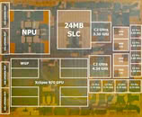 For Samsung, this is a significant launch as the company tests the limits of its SF2 2 nm node with a highly heterogeneous design. It's also a big launch for AMD since the GPU is possibly RDNA 5, about which we haven't had much information for a while. Externally, Samsung connects the Exynos 2700 with a 24-bit LPDDR6 connection, ensuring satisfactory bandwidth for both CPU and GPU core clusters. We are awaiting the first benchmarks of this mobile SoC, which could give us a preview of what the desktop RDNA 5 will be capable of.
Source:
SemiAnalysis
On the CPU front, Samsung uses Arm's off-the-shelf CPU core IP, which includes C2-Ultra and C2-Pro. This setup features a single C2-Ultra big core running at 4.24 GHz, one C2-Ultra running at 3.36 GHz, four C2-Pro cores running at 3.74 GHz, and four C2-Pro cores running at 2.88 GHz, making a total of 10 CPU cores. On the GPU side, the Xclipse 970 packs eight GPU WGPs, each containing two Compute Units. This results in 16 CUs on the GPU front if everything remains the same with RDNA 5 and no changes to the WGP/CU ratio have been made by AMD since the last-generation RDNA 4.

10 Comments on Possible AMD RDNA 5 GPU IP Ships Inside a Samsung SoC on 2 nm Node
Anyway, it will be interesting to see performance, clocks and power consumption of that GPU.I wonder if AMD could choose this node for the RDNA5 GPUs. I mean if they already have one - whatever GPU - made in this node, isn't this also a nice test vehicle for RDNA5 manufacturing?
A single DDR6 channel will be 96-bit. It's going to be quite the upgrade.
even title is lets get around being sued legal speak.
That’s interesting