Report an Error


AMD Hainan

Hainan

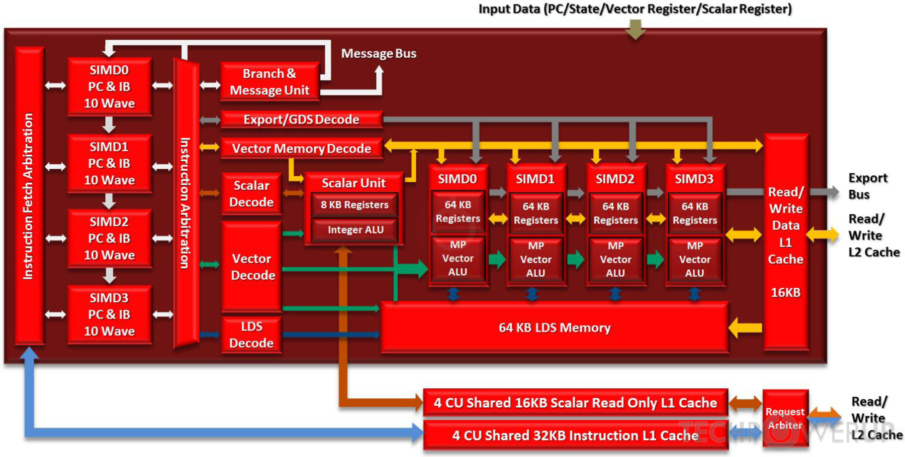
Block Diagram
CU Diagram
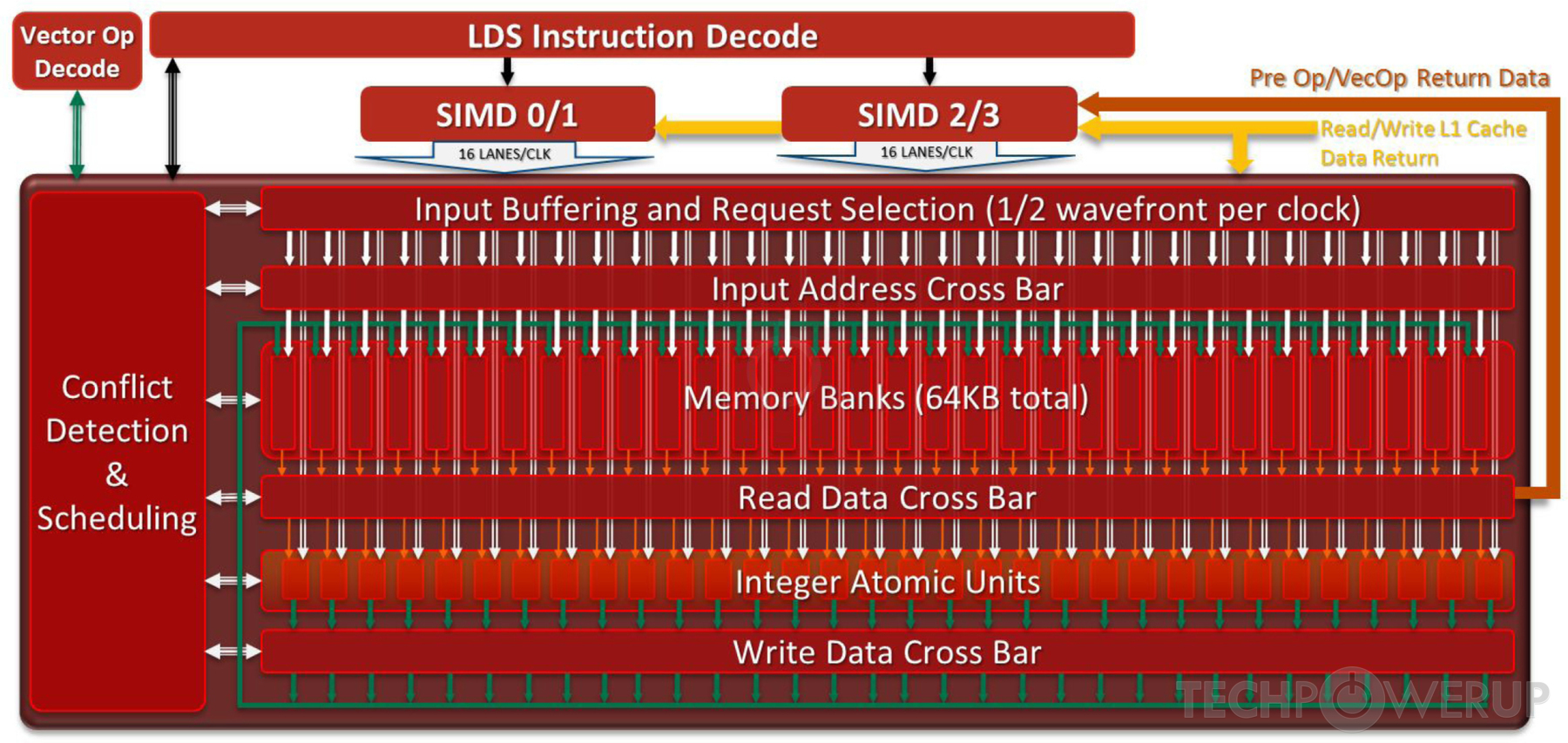
LDS Diagram
AMD's Hainan GPU uses the GCN 1.0 architecture and is made using a 28 nm production process at TSMC. With a die size of 56 mm² and a transistor count of 690 million it is a very small chip. Hainan supports DirectX 12 (Feature Level 11_1). For GPU compute applications, OpenCL version 2.1 (1.2) can be used. Unknown texture mapping units and Unknown ROPs. Due to the lack of unified shaders you will not be able to run recent games at all (which require unified shader/DX10+ support).
Further reading:
GCN 1.0 Architecture Whitepaper  , Sea Islands Instruction Set Architecture
Graphics Processor
- Released
- Unknown
- GPU Name
- Hainan
- Mobile Variant
- Sun / Jet / Exo
- Mobile Variant 2
- Banks
- Generation
- Sea Islands
- Architecture
- GCN 1.0
- Foundry
- TSMC
- Process Size
- 28 nm
- Transistors
- 690 million
- Density
- 12.3M / mm²
- Die Size
- 56 mm²
- Package
- FCBGA-962
Graphics Features
- DirectX
- 12 (11_1)
- OpenGL
- 4.6
- OpenCL
- 2.1 (1.2)
- Vulkan
- 1.2.170
- Shader Model
- 6.5 (5.1)
- WDDM
- 2.7
- Compute
- GFX6 (gfx601)
- DCE
- No Support
- UVD
- No Support
- VCE
- No Support
- CLRX
- GCN 1.0.0
Render Config
- Pixel Shaders
- Unknown
- Vertex Shaders
- Unknown
- TMUs
- Unknown
- ROPs
- Unknown
- ACEs
- 2
- GEs
- 1
All GCN 1.0 GPUs
AMD GPU Architecture History
- 2023 CDNA 3.0
- 2022-2024 RDNA 3.0
- 2021 CDNA 2.0
- 2020 CDNA 1.0
- 2020-2023 RDNA 2.0
- 2019-2020 RDNA 1.0
- 2018-2022 GCN 5.1
- 2017-2020 GCN 5.0
- 2016-2020 GCN 4.0
- 2014-2019 GCN 3.0
- 2013-2017 GCN 2.0
- 2011-2020 GCN 1.0
- 2010-2013 TeraScale 3
- 2009-2015 TeraScale 2
- 2005-2013 TeraScale
- 2005-2007 Ultra-Threaded SE
Hainan GPU Notes
| Generation: Sea Islands Mobile Variant: Sun / Jet / Exo / Banks Graphics/Compute: GFX6 (gfx601) Display Core Engine: No Support Unified Video Decoder: No Support Video Compression Engine: No Support CLRX: GCN 1.0 |
Apr 25th, 2024 21:21 EDT
change timezone
Latest GPU Drivers
New Forum Posts
- TPU's Nostalgic Hardware Club (18465)
- Post your Speedometer 3.0 Score (36)
- Size on Disk Excessively Different than Size (9)
- Dell Workstation Owners Club (3056)
- Core PL1 + GPU PL1 + Ring EDP OTHER (10)
- Best SSD for system drive (80)
- Which new games will you be buying? (315)
- BSOD if I touch the pcache offset voltage in throttlestop (i9-13900hx lenovo pro 7i) (23)
- Alphacool CORE 1 CPU block - bulging with danger of splitting? (16)
- How to check flatness of CPUs and coolers - INK and OPTICAL INTERFERENCE methods (112)
Popular Reviews
- Fractal Design Terra Review
- Thermalright Phantom Spirit 120 EVO Review
- Corsair 2000D Airflow Review
- ASUS GeForce RTX 4090 STRIX OC Review
- NVIDIA GeForce RTX 4090 Founders Edition Review - Impressive Performance
- ASUS GeForce RTX 4090 Matrix Platinum Review - The RTX 4090 Ti
- MSI GeForce RTX 4090 Suprim X Review
- Gigabyte GeForce RTX 4090 Gaming OC Review
- MSI GeForce RTX 4090 Gaming X Trio Review
- MSI GeForce RTX 4090 Suprim Liquid X Review
Controversial News Posts
- Sony PlayStation 5 Pro Specifications Confirmed, Console Arrives Before Holidays (117)
- Windows 11 Now Officially Adware as Microsoft Embeds Ads in the Start Menu (107)
- NVIDIA Points Intel Raptor Lake CPU Users to Get Help from Intel Amid System Instability Issues (106)
- AMD "Strix Halo" Zen 5 Mobile Processor Pictured: Chiplet-based, Uses 256-bit LPDDR5X (101)
- US Government Wants Nuclear Plants to Offload AI Data Center Expansion (98)
- AMD's RDNA 4 GPUs Could Stick with 18 Gbps GDDR6 Memory (88)
- Developers of Outpost Infinity Siege Recommend Underclocking i9-13900K and i9-14900K for Stability on Machines with RTX 4090 (85)
- Windows 10 Security Updates to Cost $61 After 2025, $427 by 2028 (84)