Thursday, May 9th 2019

Intel Switches Gears to 7nm Post 10nm, First Node Live in 2021
Intel's semiconductor manufacturing business has had a terrible past 5 years as it struggled to execute its 10 nanometer roadmap forcing the company's processor designers to re-hash the "Skylake" microarchitecture for 5 generations of Core processors, including the upcoming "Comet Lake." Its truly next-generation microarchitecture, codenamed "Ice Lake," which features a new CPU core design called "Sunny Cove," comes out toward the end of 2019, with desktop rollouts expected 2020. It turns out that the 10 nm process it's designed for, will have a rather short reign at Intel's fabs. Speaking at an investor's summit on Wednesday, Intel put out its silicon fabrication roadmap that sees an accelerated roll-out of Intel's own 7 nm process.
When it goes live and fit for mass production some time in 2021, Intel's 7 nm process will be a staggering 3 years behind TSMC, which fired up its 7 nm node in 2018. AMD is already mass-producing CPUs and GPUs on this node. Unlike TSMC, Intel will implement EUV (extreme ultraviolet) lithography straightaway. TSMC began 7 nm with DUV (deep ultraviolet) in 2018, and its EUV node went live in March. Samsung's 7 nm EUV node went up last October. Intel's roadmap doesn't show a leap from its current 10 nm node to 7 nm EUV, though. Intel will refine the 10 nm node to squeeze out energy-efficiency, with a refreshed 10 nm+ node that goes live some time in 2020.


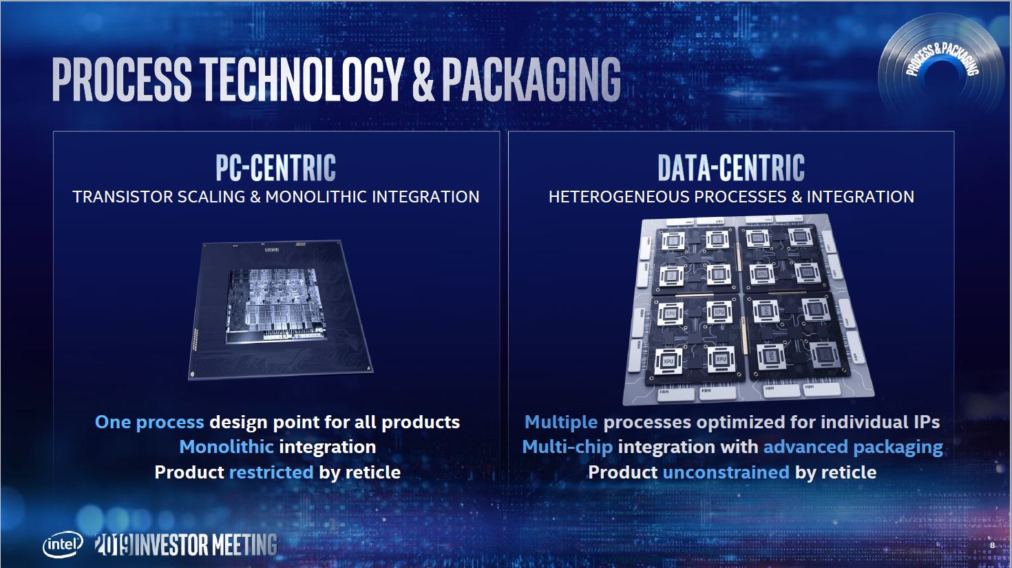
 The transition from 10 nm+ to 7 nm EUV will significantly increase transistor-densities. Intel is also making the manufacturing process efficient, by reducing "design rules" by 4 times, giving chip-designers more flexibility and creative freedom in the way they design nanoscopic circuitry. The process will also be optimized for heterogeneous chip designs, Foveros packaging (a very advanced form of MCM), and EMIB (reduced footprint interposer).
The 7 nm EUV node will receive two major updates in quick succession. The 7 nm+ node is slated for 2022, and succeeding 7 nm++ node in 2023. Intel did not detail the two besides illustrating performance/Watt gains by almost as much as the transition from 10 nm+ to 7 nm. Elsewhere in the market, the early 2020s could see TSMC 6 nm EUV take center-stage, and Samsung implement its 5 nm EUV node.
 Intel will build an Xe enterprise GPGPU based on 7 nm EUV for market release in 2021. The company was specific in mentioning that an "enterprise GP-GPU" will be built on it, and not its entire Xe lineup that includes client-segment, professional, and cloud GPUs. The Xe discrete GPU team, led by Raja Koduri, is probably making a ropewalk, by giving Intel "something" to build on its own fabs, while seeking out Samsung's cutting-edge 5 nm EUV node for the rest of its lineup. Intel confirmed that the its first 7 nm product will be a GPGPU, followed closely by a server CPU.
Source:
AnandTech
When it goes live and fit for mass production some time in 2021, Intel's 7 nm process will be a staggering 3 years behind TSMC, which fired up its 7 nm node in 2018. AMD is already mass-producing CPUs and GPUs on this node. Unlike TSMC, Intel will implement EUV (extreme ultraviolet) lithography straightaway. TSMC began 7 nm with DUV (deep ultraviolet) in 2018, and its EUV node went live in March. Samsung's 7 nm EUV node went up last October. Intel's roadmap doesn't show a leap from its current 10 nm node to 7 nm EUV, though. Intel will refine the 10 nm node to squeeze out energy-efficiency, with a refreshed 10 nm+ node that goes live some time in 2020.


The 7 nm EUV node will receive two major updates in quick succession. The 7 nm+ node is slated for 2022, and succeeding 7 nm++ node in 2023. Intel did not detail the two besides illustrating performance/Watt gains by almost as much as the transition from 10 nm+ to 7 nm. Elsewhere in the market, the early 2020s could see TSMC 6 nm EUV take center-stage, and Samsung implement its 5 nm EUV node.


23 Comments on Intel Switches Gears to 7nm Post 10nm, First Node Live in 2021
Even Raja doesn't trust Intel foundry, so he's designing a token Xe product (a Larrabee-like GPGPU accelerator) for Intel 7 nm EUV, while every other Xe GPU will be built on Samsung 5 nm EUV.
TSMC intends their 5nm to start volume production in the end of 2020.
Edit:So, point by point:
1. Intel 7nm (mass production 2021) is comparable to TSMC 5nm (volume production end of 2020). That is on 4th slide as well.
2. Intel has no choice when it comes to EUV due to feature sizes on a small node. 7nm (and Intel's 10nm) are right on the line where not using EUV is still feasible but barely. Both TSMC and Samsung are starting to partially use EUV on 7nm (7nm+ for TSMC and Samsung right away). EUV has some teething problems, technical side of things has been mostly worked out but tooling availability is still a problem and things just take time.
3. Intel's roadmap is curious, both in terms of foundry and CPUs. Looks like there will be very limited Intel 10nm and despite fast 10nm iterations they intend to largely skip it and shoot for 7nm in 2021. This makes perfect sense both financially as well as technically. Setting up foundries for a node is expensive (billions, with a B) and time consuming. If the intended lifetime of a node is about a year before the next one is ready, it would not make much sense to widely adopt the node.
TSMC is using EUV on 4 non-critical layers on their 7nm+ node. They have not been very specific but 5nm is going to use - at least mostly, if not completely - EUV. The intermediate 6nm seems to be in large part just from extended use of EUV on otherwise 7nm node. Samsung is following largely the same path except they skipped doing 7nm without any EUV.
By the way, what is ITRS spec for 7nm? Quick Google didn't give me a proper answer, hoping you have a link at hand :)
Reading more and more about their 10nm fiasco, it seems a lot of the issue was that Intel needed EUV to make it actually work, but the technology literally wasn't available. So they were forced to attempt to implement the far-more-complex multi-patterning... which has finally come right, just in time for EUV to be practical. Well, that's the risk of being a tech leader; sometimes you are forced to take detours, and sometimes those detours end up being dead ends.
Don't think this qualifies as a paper launch.
For now, intel states that "is nearly ready to ship 10-nanometer processors in large volumes "... in June.
www.techpowerup.com/250549/intel-demoes-sunnycove-high-performance-core
If you WANT it to be crappy, that's a whole different thing, but it's not much to make an assumption out of. :D If anything, I'm a AMD fan myself, and I'd like to see AMD take some of the CPU market share, but this isn't a paper launch. You need model numbers, price, launch dates, performance tests and maybe even reviews for that.
It may still be crap, but we have zero evidence that it is. The fact that Intel stayed at 4 core and 14 nm forever, or changes the socket too often, or sells multiplier locked CPU's, or calls the 9900K a 95 W SKU isn't evidence for Ice Lake being crap.
For the record;
Intel was first to ship a product on this generation of nodes in April 2018 followed by AMD in ~December 2018, but neither have shipped volumes yet. But at least AMD have shipped the largest chip so far, and both expect to ship "volumes" in Q3 2019.
I think that desktops will never see a 10 nm product, cause Comet Lake will launch in Q1 2020 and Rocket Lake in Q1 2021 both using 14 nm, Golden Cove would launch at the end of 2021 in 7 nm for desktop. So desktops will skip both Ice Lake and Tiger Lake in 10 nm (and Cannon Lake which by now is more than certain that is dropped).irds.ieee.org/images/files/pdf/2017/2017IRDS_MM.pdf page 12
fuse.wikichip.org/news/2004/iedm-2018-intels-10nm-standard-cell-library-and-power-delivery/4