Monday, January 6th 2020

Xbox Head Posts "Project Scarlett" (Xbox Series X) SoC Picture, Has that 7nm Tinge
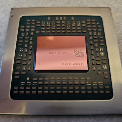
Phil Spencer, head of the Xbox division at Microsoft, posted a picture of the semi-custom SoC at the heart of the company's upcoming "Project Scarlett" Xbox Series X game console as his Twitter avatar. The picture reveals a chip that looks visibly similar to that of "Project Scorpio" (Xbox One X). The picture was also taken from an angle that reveals the pinkish/auburn tinge of 7 nm AMD chips made at TSMC. You'll find the same tinge on chips such as "Navi 10" when viewed from an angle. The die unabashedly bears the "Project Scarlett" and "8K" markings.
Next-generation game consoles are marketing 4K 60 Hz and 8K gaming capability. They likely use a combination of dynamic resolution-scale and variable rate shading to achieve this. The "Project Scarlett" SoC is a semi-custom chip co-designed by Microsoft and AMD, and uses CPU cores based on the company's "Zen 2" microarchitecture, combined with a powerful GPU based on RDNA2, which features hardware-accelerated ray-tracing and variable-rate shading. Hardware enthusiasts on Twitter are abuzz with estimating the die-size of the SoC, with calculations pinning it around the 350 mm² mark ±10 mm², or roughly similar to that of "Project Scorpio," but one must factor in the switch to 7 nm from 16 nm significantly increasing transistor-density.
Source:
Phil Spencer (Twitter)
Next-generation game consoles are marketing 4K 60 Hz and 8K gaming capability. They likely use a combination of dynamic resolution-scale and variable rate shading to achieve this. The "Project Scarlett" SoC is a semi-custom chip co-designed by Microsoft and AMD, and uses CPU cores based on the company's "Zen 2" microarchitecture, combined with a powerful GPU based on RDNA2, which features hardware-accelerated ray-tracing and variable-rate shading. Hardware enthusiasts on Twitter are abuzz with estimating the die-size of the SoC, with calculations pinning it around the 350 mm² mark ±10 mm², or roughly similar to that of "Project Scorpio," but one must factor in the switch to 7 nm from 16 nm significantly increasing transistor-density.
16 Comments on Xbox Head Posts "Project Scarlett" (Xbox Series X) SoC Picture, Has that 7nm Tinge
Scorpio had 2560 SPs with 2 CUs disabled and while the Xbox Scarlett APU is clearly bigger, it is not possible to speculate based just on the die size because of the different process node involved (7nm vs 16nm) but we can safely say that you are looking at at least 50% more power in the same die space. Since the Scorpio APU can output roughly 6 TFLOPs of power, we can guesstimate a range of at least 9 TFLOPs for the Scarlett APU ( up to 12 TFLOPS is within the realm of possibility).
Tbf i was shocked n awed by the geeky chip shot, so much so i forgot to read, niiice.
It could render 2D games at 8K but vast majority of them will be 4K.