News Posts matching #Die

Return to Keyword Browsing

MediaTek Launches Next-gen ASIC Design Platform with Co-packaged Optics Solutions

Ahead of the 2024 Optical Fiber Communication Conference (OFC), MediaTek (last week) announced it is launching a next-generation custom ASIC design platform that includes the heterogeneous integration of both high-speed electrical and optical I/Os in the same ASIC implementation. MediaTek will be demonstrating a serviceable socketed implementation that combines 8x800G electrical links and 8x800G optical links for a more flexible deployment. It integrates both MediaTek's in-house SerDes for electrical I/O as well as co-packaged Odin optical engines from Ranovus for optical I/O. Leveraging the heterogeneous solution that includes both 112G LR SerDes and optical modules, this CPO demonstration delivers reduced board space and device costs, boosts bandwidth density, and lowers system power by up to 50% compared to existing solutions.

Additionally, Ranovus' Odin optical engine has the option to provide either internal or external laser optical modules to better align with practical usage scenarios. MediaTek's ASIC experience and capabilities in the 3 nm advanced process, 2.5D and 3D advanced packaging, thermal management, and reliability, combined with optical experience, makes it possible for customers to access the latest technology for high-performance computing (HPC), AI/ML and data center networking.

Intel Lunar Lake-MX to Embed Samsung LPDDR5X Memory on SoC Package

According to sources close to Seoul Economy, and reported by DigiTimes, Intel has reportedly chosen Samsung as a supplier for its next-generation Lunar Lake processors, set to debut later this year. The report notes that Samsung will provide LPDDR5X memory devices for integration into Intel's processors. This collaboration could be a substantial win for Samsung, given Intel's projection to distribute millions of Lunar Lake CPUs in the coming years. However, it's important to note that this information is based on a leak and has not been officially confirmed. Designed for ultra-portable laptops, the Lunar Lake-MX platform is expected to feature 16 GB or 32 GB of LPDDR5X-8533 memory directly on the processor package. This on-package memory approach aims to minimize the platform's physical size while enhancing performance over traditional memory configurations. With Lunar Lake's exclusive support for on-package memory, Samsung's LPDDR5X-8533 products could significantly boost sales.

While Samsung is currently in the spotlight, it remains unclear if it will be the sole LPDDR5X memory provider for Lunar Lake. Intel's strategy involves selling processors with pre-validated memory, leaving the door open for potential validation of similar memory products from competitors like Micron and SK Hynix. Thanks to a new microarchitecture, Intel has promoted its Lunar Lake processors as a revolutionary leap in performance-per-watt efficiency. The processors are expected to utilize a multi-chipset design with Foveros technology, combining CPU and GPU chipsets, a system-on-chip tile, and dual memory packages. The CPU component is anticipated to include up to eight cores, a mix of four high-performance Lion Cove and four energy-efficient Skymont cores, alongside advanced graphics, cache, and AI acceleration capabilities. Apple's use of on-package memory in its M-series chips has set a precedent in the industry, and with Intel's Lunar Lake MX, this trend could extend across the thin-and-light laptop market. However, systems requiring more flexibility in terms of configuration, repair, and upgrades will likely continue to employ standard memory solutions like SODIMMs and/or the new CAMM2 modules that offer a balance of high performance and energy efficiency.

SSD Overclocking? It can be Done, with Serious Performance Gains

The PC master race has yielded many interesting activities for enthusiasts alike, with perhaps the pinnacle of activities being overclocking. Usually, subjects for overclocking include CPUs, GPUs, and RAM, with other components not actually being capable of overclocking. However, the enthusiast force never seems to settle, and today, we have proof of overclocking an off-the-shelf 2.5-inch SATA III NAND Flash SSD thanks to Gabriel Ferraz, a Computer Engineering graduate, and TechPowerUp's SSD database maintainer. He uses the RZX Pro 256 GB SSD in the video, a generic NAND Flash drive. The RZX Pro uses the Silicon Motion SM2259XT2 single-core, 32-bit ARC CPU running up to 550 MHz. It has two channels at 400 MHz, each with eight chip enable interconnects, allowing up to 16 NAND Flash dies to operate. The SSD doesn't feature a DRAM cache or support a host memory buffer. It has only one NAND Flash memory chip from Kioxia, uses BiCS FLASH 4 architecture, has 96 layers, and has 256 GB capacity.

While this NAND Flash die is rated for up to 400 MHz or 800 MT/s, it only ran at less than half the speed at 193.75 MHz or 387.5 MT/s at default settings. Gabriel acquired a SATA III to USB 3.0 adapter with a JMS578 bridge chip to perform the overclock. This adapter allows hot swapping of SSDs without the need to turn off the PC. He shorted two terminals in the drive's PCB to get the SSD to operate without its default safe mode. Mass Production Tools (MPTools), which OEMs use to flash SSDs, were used to change the firmware settings. Each NAND Flash architecture has its own special version of MPTools. The software directly shows control of the Flash clock, CPU clock, and output driving. However, additional tweaks like Flash IO driving with subdivisions need modifications. Control and Flash On-Die Termination (ODT) and Schmitt window trigger (referring to the Schmitt trigger comparator circuit) also needed a few modifications to make it work.
EK Shows Nucleus AIO CR360 for Direct-Die Water Cooling at CES 2024

During the CES 2024 show, EK unveiled an exciting new addition to their premium all-in-one (AIO) CPU cooler lineup—the EK-Nucleus AIO CR360 Direct Die D-RGB. As the name suggests, this new 360 mm AIO water cooler is purpose-built for direct die cooling of delidded Intel LGA1700 CPUs. The EK-Nucleus Direct Die stands out with its custom cold plate and mounting mechanism, which are exclusively engineered for exposed CPU dies. The nickel-plated copper base ensures compatibility with liquid metal TIMs like the included Thermal Grizzly Conductonaut, which comes in the package. EK has worked with der8auer to provide delidding service kits and tools to facilitate easy DIY removal of the integrated heat spreader (IHS).

The package also contains a contact frame and protective foam for safe liquid metal application. At the heart of the cooler is a powerful AIO pump EK co-developed with the OEM manufacturer, meaning it is not an off-the-shelf pump found in other AIOs and is capable of up to 500 L/h flow rate. The reinforced, sleeved rubber tubing is fitted with aluminium covers for durability. Integrated omnilink connectors allow daisy chaining of the three included 120 mm D-RGB fans for cable management. The EK-Nucleus Direct Die offers extensive RGB lighting customization with illuminated circle accents on the removable pump top covers. The diamond-cut brushed aluminium side panels and radiator cowl add to the premium aesthetic. The new AIO will be available for the Intel LGA1700 platform, with hopefully more versions later. The EK-Nucleus AIO CR360 Direct Die D-RGB is now available for pre-order at €202.90 MSRP price tag.
Intel "Emerald Rapids" Die Configuration Leaks, More Details Appear

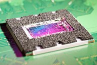
Thanks to the leaked slides obtained by @InstLatX64, we have more details and some performance estimates about Intel's upcoming 5th Generation Xeon "Emerald Rapids" CPUs, boasting a significant performance leap over its predecessors. Leading the Emerald Rapids family is the top-end SKU, the Xeon 8592+, which features 64 cores and 128 threads, backed by a massive 480 MB L3 cache pool. The upcoming lineup shifts from a 4-tile to a 2-tile design to minimize latency and improve performance. The design utilizes the P-Core architecture under the Raptor Cove ISA and promises up to 40% faster performance than the current 4th Generation "Sapphire Rapids" CPUs in AI applications utilizing Intel AMX engine. Each chiplet has 35 cores, three of which are disabled, and each tile has two DDR5-5600 MT/s memory controllers, which operate two memory channels each and translating that into eight-channel design. There are three PCIe controllers per die, making it six in total.
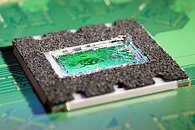
Newer protocols and AI accelerators also back the upcoming lineup. Now, the Emerald Rapids family supports the Compute Express Link (CXL) Types 1/2/3 in addition to up to 80 PCIe Gen 5 lanes and enhanced Intel Ultra Path Interconnect (UPI). There are four UPI controllers spread over two dies. Moreover, features like the four on-die Intel Accelerator Engines, optimized power mode, and up to 17% improvement in general-purpose workloads make it seem like a big step up from the current generation. Much of this technology is found on the existing Sapphire Rapids SKUs, with the new generation enhancing the AI processing capability further. You can see the die configuration below. The 5th Generation Emerald Rapids designs are supposed to be official on December 14th, just a few days away.

Synopsys and TSMC Streamline Multi-Die System Complexity with Unified Exploration-to-Signoff Platform and Proven UCIe IP on TSMC N3E Process

Synopsys, Inc. today announced it is extending its collaboration with TSMC to advance multi-die system designs with a comprehensive solution supporting the latest 3Dblox 2.0 standard and TSMC's 3DFabric technologies. The Synopsys Multi-Die System solution includes 3DIC Compiler, a unified exploration-to-signoff platform that delivers the highest levels of design efficiency for capacity and performance. In addition, Synopsys has achieved first-pass silicon success of its Universal Chiplet Interconnect Express (UCIe) IP on TSMC's leading N3E process for seamless die-to-die connectivity.

"TSMC has been working closely with Synopsys to deliver differentiated solutions that address designers' most complex challenges from early architecture to manufacturing," said Dan Kochpatcharin, head of the Design Infrastructure Management Division at TSMC. "Our long history of collaboration with Synopsys benefits our mutual customers with optimized solutions for performance and power efficiency to help them address multi-die system design requirements for high-performance computing, data center, and automotive applications."

NVIDIA Blackwell GB100 Die Could Use MCM Packaging

NVIDIA's upcoming Blackwell GPU architecture, expected to succeed the current Ada Lovelace architecture, is gearing up to make some significant changes. While we don't have any microarchitectural leaks, rumors are circulating that Blackwell will have different packaging and die structures. One of the most intriguing aspects of the upcoming Blackwell is the mention of a Multi-Chip Module (MCM) design for the GB100 data-center GPU. This advanced packaging approach allows different GPU components to exist on separate dies, providing NVIDIA with more flexibility in chip customization. This could mean that NVIDIA can more easily tailor its chips to meet the specific needs of various consumer and enterprise applications, potentially gaining a competitive edge against rivals like AMD.

While Blackwell's release is still a few years away, these early tidbits paint a picture of an architecture that isn't just an incremental improvement but could represent a more significant shift in how NVIDIA designs its GPUs. NVIDIA's potential competitor is AMD's upcoming MI300 GPU, which utilized chiplets in its designs. Chiplets also provide ease of integration as smaller dies provide better wafer yields, meaning that it makes more sense to switch to smaller dies and utilize chiplets economically.

Tachyum Achieves 192-Core Chip After Switch to New EDA Tools

Tachyum today announced that new EDA tools, utilized during the physical design phase of the Prodigy Universal Processor, have allowed the company to achieve significantly better results with chip specifications than previously anticipated, after the successful change in physical design tools - including an increase in the number of Prodigy cores to 192.

After RTL design coding, Tachyum began work on completing the physical design (the actual placement of transistors and wires) for Prodigy. After the Prodigy design team had to replace IPs, it also had to replace RTL simulation and physical design tools. Armed with a new set of EDA tools, Tachyum was able to optimize settings and options that increased the number of cores by 50 percent, and SERDES from 64 to 96 on each chip. Die size grew minimally, from 500mm2 to 600mm2 to accommodate improved physical capabilities. While Tachyum could add more of its very efficient cores and still fit into the 858mm2 reticle limit, these cores would be memory bandwidth limited, even with 16 DDR5 controllers running in excess of 7200MT/s. Tachyum cores have much higher performance than any other processor cores.

Samsung Electronics Announces Second Quarter 2023 Results

Samsung Electronics today reported financial results for the second quarter ended June 30, 2023. The Company posted KRW 60.01 trillion in consolidated revenue, a 6% decline from the previous quarter, mainly due to a decline in smartphone shipments despite a slight recovery in revenue of the DS (Device Solutions) Division. Operating profit rose sequentially to KRW 0.67 trillion as the DS Division posted a narrower loss, while Samsung Display Corporation (SDC) and the Digital Appliances Business saw improved profitability.

The Memory Business saw results improve from the previous quarter as its focus on High Bandwidth Memory (HBM) and DDR5 products in anticipation of robust demand for AI applications led to higher-than-guided DRAM shipments. System semiconductors posted a decline in profit due to lower utilization rates on weak demand from major applications.

Synopsys, TSMC and Ansys Strengthen Ecosystem Collaboration to Advance Multi-Die Systems

Accelerating the integration of heterogeneous dies to enable the next level of system scalability and functionality, Synopsys, Inc. (Nasdaq: SNPS) has strengthened its collaboration with TSMC and Ansys for multi-die system design and manufacturing. Synopsys provides the industry's most comprehensive EDA and IP solutions for multi-die systems on TSMC's advanced 7 nm, 5 nm and 3 nm process technologies with support for TSMC 3DFabric technologies and 3Dblox standard. The integration of Synopsys implementation and signoff solutions and Ansys multi-physics analysis technology on TSMC processes allows designers to tackle the biggest challenges of multi-die systems, from early exploration to architecture design with signoff power, signal and thermal integrity analysis.

"Multi-die systems provide a way forward to achieve reduced power and area and higher performance, opening the door to a new era of innovation at the system-level," said Dan Kochpatcharin, head of Design Infrastructure Management Division at TSMC. "Our long-standing collaboration with Open Innovation Platform (OIP) ecosystem partners like Synopsys and Ansys gives mutual customers a faster path to multi-die system success through a full spectrum of best-in-class EDA and IP solutions optimized for our most advanced technologies."

AMD's Zen 4 I/O Die Detailed Courtesy of ISSCC Presentation

Although we've known most of the details of AMD's I/O die in its Zen 4 processors, until now, AMD hadn't shared a die shot of the cIOD, but thanks to its ISSCC 2023 presentation, we not only have a die shot of the cIOD, but some friendly people on the internet have also made annotations for us mere mortals. There are no big secrets here, but based on the annotations by @Locuza_ we now know for certain that it's not possible to use the current I/O die with three CCDs, as it only has two GMI3 interfaces, to which the CCDs are connected.

If you're wondering about the 2x 40-bit memory interface, it's for ECC memory support outside of the on-die ECC support of DDR5 memory. Also note that DDR5 memory is two times 32-bit in non ECC mode. That said, it's up to the motherboard makers to implement support for ECC memory, but it would appear all Zen 4 CPUs support it. The addition of a GPU, even a basic one like this, takes up a fair bit of space inside the cIOD, especially once you add things like video decoders/encoders and so on. In fact, it appears that the parts related to the GPU and video decoders/encoders take up at least a third of the space inside the I/O die, yet thanks to a significant die shrink from the Zen 3 era cIOD, it's physically smaller in the Zen 4 processors, while having an estimated 58 percent increase in transistors.

AMD Ryzen 5 5600G APU Die Shots Published

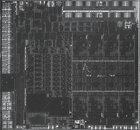
We have recently seen the first high-resolution die shots of AMD's Ryzen 5 5600G Cezanne APU thanks to the work of Fritzchens Fritz. The photos show the internal layout of the processor with its Zen 3 CPU, Vega GPU, and corresponding components. To get these shots, the chip had to be delidded by removing the IHS which has been made harder with the move to a soldered design. The Ryzen 5 5600G is a 6 core, 12 thread part with 7 Vega GPU cores which can all be seen in the annotated diagram of the die created by Locuza. The diagram also shows the suspected locations of various PCIe 3.0, and memory controllers along with cache placements for the CPU and GPU. The processor is manufactured on TSMC's 7 nm process and features a total of 10.7 Billion transistors packed into the 180 mm² die.

AMD "Milan-X" Processor Could Use Stacked Dies with X3D Packaging Technology

AMD is in a constant process of processor development, and there are always new technologies on the horizon. Back in March of 2020, the company has revealed that it is working on new X3D packaging technology, that integrated both 2.5D and 3D approaches to packing semiconductor dies together as tightly as possible. Today, we are finally getting some more information about the X3D technology, as we have the first codename of the processor that is featuring this advanced packaging technology. According to David Schor, we have learned that AMD is working on a CPU that uses X3D tech with stacked dies, and it is called Milan-X.

The Milan-X CPU is AMD's upcoming product designed for data center usage. The rumors suggest that the CPU is designed for heavy bandwidth and presumably a lot of computing power. According to ExecutableFix, the CPU uses a Genesis-IO die to power the connectivity, which is an IO die from EPYC Zen 3 processors. While this solution is in the works, we don't know the exact launch date of the processor. However, we could hear more about it in AMD's virtual keynote at Computex 2021. For now, take this rumor with a grain of salt.
AMD X3D Packaging Technology

Sony Playstation 5 SoC Die Has Been Pictured

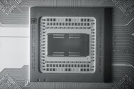
When AMD and Sony collaborated on making the next generation console chip, AMD has internally codenamed it Flute, while Sony codenamed it Oberon or Ariel. This PlayStation 5 SoC die has today been pictured thanks to the Fritzchens Fritz and we get to see a closer look at the die internals. Featuring eight of AMD's Zen2 cores that can reach frequencies of up to 3.5 GHz, the CPU is paired with 36 CU GPU based on the RDNA 2 technology. The GPU is capable of running at speed of up to 2.23 GHz. The SoC has been made to accommodate all of that hardware, and bring IO to connect it all.

When tearing down the console, the heatsink and the SoC are connected by liquid metal, which is used to achieve the best possible heat transfer between two surfaces. Surrounding the die there is a small amount of material used to prevent liquid metal (a conductive material) from possibly spilling and shorting some components. Using a special short wave infrared light (SWIR) microscope, we can take a look at what is happening under the hood without destroying the chip. And really, there are a few distinct areas that are highlighted by the Twitter user @Locuza. As you can see, the die has special sectors with the CPU complex and a GPU matrix with plenty of workgroups and additional components for raytracing.

AMD Ryzen 5000 Cezanne APU Die Render Leaked

VideoCardz has recently received a render of the upcoming AMD Ryzen 5000 Cezanne APU which is expected to be unveiled next week. The Zen 3 Cezanne APUs support up to 8 cores and 16 threads just like Zen 2 Renoir APUs. The Cezanne APU should support up to 8 graphics cores and 20 PCIe lanes, it is currently unknown whether these lanes will be PCIe 3.0 or PCIe 4.0. The Cezanne die appears to be ~10% larger than Renoir which comes from the larger Zen 3 core design and a larger L3 cache of 16 MB. The new Ryzen 5000H Cezanne series processors are expected to be announced by AMD next week and will power upcoming low and high power laptops.

Apple A14 SoC Put Under the Microscope; Die Size, and Transistor Density Calculated

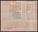
Apple has established itself as a master of silicon integrated circuit design and has proven over the years that its processors deliver the best results, generation after generation. If we take a look at the performance numbers of the latest A14 Bionic, you can conclude that its performance is now rivaling some of the x86_64 chips. So you would wonder, what is inside this SoC that makes it so fast? That is exactly what ICmasters, a semiconductor reverse engineering and IP services company, has questioned and decided to find out. For starters, we know that Apple manufactures the new SoCs on TSMC's N5 5 nm node. The Taiwanese company promises to pack 171.3 million transistors per square millimeter, so how does it compare to an actual product?

ICmasters have used electron microscopy to see what the chip is made out of and to measure the transistor density. According to this source, Apple has a chip with a die size of 88 mm², which packs 11.8 billion N5 transistors. The density metric, however, doesn't correspond to that of TSMC. Instead of 171.3 million transistors per mm², the ICmasters measured 134.09 million transistors per mm². This is quite a difference, however, it is worth noting that each design will have it different due to different logic and cache layout.
Apple A14 SoC Die Apple A14 SoC

Samsung Starts Offering First A-Die Based RAM

Samsung's B die has been widely known as a good, high performance variant of DRAM memory, loved by overclockers because of its ability to get to a high frequency with relatively low timings. However, B die has been discontinued and now Samsung started offering its replacement in form of the newly developed A die manufactured in 1z nm (1z class) lithography process. Despite the lack of technical details surrounding the new die type, Hardwareluxx has received a tip from its reader about new RAM offering that incorporates A die memory.

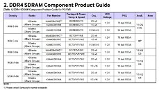
The M378A4G43AB2-CVF, as it is called in the listing, is a 32 GB, single dimm DDR4 RAM with operating speed of 2933 MHz and CL21-21-21 timings. This particular offer isn't something to be excited about as the frequency is good, but the timings are quite high for that speed. Given that we don't know where the A die is targeted at, we can speculate that its current aim is at mid-tier systems, where the mediocre performance is okay and the system isn't suffering (performance wise) because of it. Nonetheless this find is quite interesting as it gives first hints at what can we expect in therms of future A die DRAM offerings. Remember, it took some time for B die as well to get to the level of performance we have today, so it is entirely possible that A die will improve and try to aim for greater performance level than it currently has.

Samsung Launches Sixth Generation 3D V-NAND SSDs

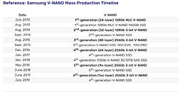
Samsung Electronics, the world leader in advanced memory technology, today announced that it has begun mass producing 250-gigabyte (GB) SATA solid state drive (SSD) that integrates the company's sixth-generation (1xx-layer) 256-gigabit (Gb) three-bit V-NAND for global PC OEMs. By launching a new generation of V-NAND in just 13 months, Samsung has reduced the mass production cycle by four months while securing the industry's highest performance, power efficiency and manufacturing productivity.

"By bringing cutting-edge 3D memory technology to volume production, we are able to introduce timely memory lineups that significantly raise the bar for speed and power efficiency," said Kye Hyun Kyung, executive vice president of Solution Product & Development at Samsung Electronics. "With faster development cycles for next-generation V-NAND products, we plan to rapidly expand the markets for our high-speed, high-capacity 512 Gb V-NAND-based solutions."

Samsung Kills Production of Famed B-die DDR4 Memory in Favor or Higher Densities

As the world becomes more and more centered on data, as well as its processing and storage, increased memory density across products is becoming more of a necessity. It seems that out of this necessity and a need to streamline its memory production towards favoring denser outputs, Samsung is killing of the famous B-die chips, which were - and still are - part of a love affair with any enthusiast's Ryzen desktop.

Memory compatibility issues with the first gen Ryzen took a while to dissipate, and didn't vanish entirely; however, overclockers quickly found that the most stable and overclockable memory ICs all were of the Samsung B-die type. Now, the company has updated its product catalogue to reflect EOL (End of Life) status for B-dies, replacing it with denser M-Die and A-Die products. M-dies were supposed to bring 32 GB densities to a single rank of memory - and have apparently been siphoned off to server applications and left out in the cold for consumer purchase), while the new A dies increase memory density per IC, meaning less of these are necessary to achieve the same final memory footprint. Whether or not these will feature the same Ryzen compatibility and overclockability as their B-die predecessors is unknown at this point, but it would make a lot of enthusiasts slightly unhappy - and increase the value of B-die offerings in any sort of discerning second-hand market - if they did not.

The Ncore V1 is the World's First Naked Die Cooling Waterblock for LGA1151 CPUs

The world's first waterblock designed for naked die cooling throws years of conventional wisdom out of the window. It features six unique patentable features including its "in-frame" mounting mechanism. The man behind NUDEcnc, Arek Tobiszewski has started this Kickstarter campaign in order to get a professional CNC machine, which will enable this inventor to deliver Ncore and other cool projects to the audience. He has been brave enough to send the Ncore for a review to Kyle Bennett from HardOcp; Linus tech tips; buildzoid, and Techlipton. Some of the reviews are already up, and are very promising.

Intel Skylake-X HCC CPU Delidded by Der8auer, also not Soldered

Overclocking poster-boy Der8auer has seemingly gotten his hands on some early samples of Intel's Skylake-X high core count (HCC)HEDT CPUs. The upcoming 12 to 18-core enthusiast-class CPUs are being launched on the same X299 platform on socket LGA 2066 that Intel has already launched 4 (Kaby Lake-X), 6, 8 and 10-core parts already, and are supposed to bring Intel towards a level playing field - and then some - with competitor AMD's Threadripper CPUs, which boast of up to 16 cores.

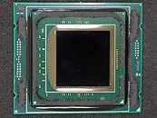
From this delidding process with Der8auer's own delidding tool, Delid-Die-Mate-X, seems to result a die that is much larger - as expected - than Intel's 10-core i9-7900X. At the same time, it seems that Intel is still opting, again, for not soldering its enthusiast-targeted CPUs, which would result in better temperatures and, potentially, overclocking potential. The fact that Der8auer managed to delid the i9-7920X and didn't recommend against doing it likely means that there is minimal risk of damaging your CPU while subjecting it to this process. This is something the renowned overclocker did do when he recommended that users shouldn't delid their Ryzen or Threadripper CPUs looking for better temperatures, since the fact that these were soldered would likely result in both catastrophic damage and a much diminished chance of operating temperatures improvement through the application of special purpose thermal compounds. The Facebook post from Der8auer with the delidded 7920X likely serves as an appetizer for an upcoming delid video on YouTube, as has been the overclocker's MO.

AMD Raja Koduri Confirms RX Vega Die Size at 484 mm²

AMD's Raja Koduri, leader of the company's Radeon Technologies Group, has somewhat informally confirmed on Twitter the overall die size of AMD's Vega chips. After PC Perspective updated their prognosis regarding Vega's die-size to a beefier 512 mm², Twitter users plied Raja Koduri with questions regarding this subject. Koduri declined to answer directly, actually opting for a somewhat cryptic response, in that " (...) the answer [to Vega's die-size] is the closest perfect square number actually:)".

For the math-savvy around here (or even just for those of you who have read the headline), that particular equation should solve towards a perfect 484 mm² die area. Good news for AMD: this isn't the company's biggest die-size in consumer GPUs ever. That dubious honor goes to the company's Fiji XT silicon which powered the company's R9 Fury X, coming in at a staggering 596 mm² in the 28 nm process. For comparison, AMD's current Polaris 20 XTX-based RX 580 chip comes in at slightly less than half the confirmed RX Vega's die-size, at a much more yield-friendly 232 mm². NVIDIA's current top-of-the-line Titan Xp comes in at a slightly smaller 471 mm² die-size.
Return to Keyword Browsing
Apr 19th, 2024 22:02 EDT change timezone

New Forum Posts

Popular Reviews

Controversial News Posts