Thursday, February 12th 2026

Samsung Ships Industry-First Commercial HBM4 With Ultimate Performance for AI Computing
Samsung Electronics Co., Ltd., a global leader in advanced memory technology, today announced that it has begun mass production of its industry-leading HBM4 and has shipped commercial products to customers. This achievement marks a first in the industry, securing an early leadership position in the HBM4 market. By proactively leveraging its most advanced 6th-generation 10 nanometer (nm)-class DRAM process (1c), the company achieved stable yields and industry-leading performance from the outset of mass production—all accomplished seamlessly and without any additional redesigns.
"Instead of taking the conventional path of utilizing existing proven designs, Samsung took the leap and adopted the most advanced nodes like the 1c DRAM and 4 nm logic process for HBM4," said Sang Joon Hwang, Executive Vice President and Head of Memory Development at Samsung Electronics. "By leveraging our process competitiveness and design optimization, we are able to secure substantial performance headroom, enabling us to satisfy our customers' escalating demands for higher performance, when they need them."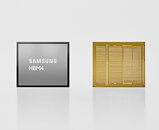 Setting the Bar for Maximum Performance and Efficiency
Samsung's HBM4 delivers a consistent processing speed of 11.7 gigabits-per-second (Gbps), exceeding the industry standard of 8 Gbps by approximately 46% and setting a new benchmark for HBM4 performance. This represents a 1.22x increase over the maximum pin speed of 9.6 Gbps of its predecessor, HBM3E. HBM4's performance can be further enhanced up to 13 Gbps, as well, effectively mitigating data bottlenecks that intensify as AI models continue to scale up.
Also, total memory bandwidth per single stack is increased by 2.7x compared to HBM3E, to a maximum of 3.3 terabytes-per-second (TB/s).
Through 12-layer stacking technology, Samsung offers HBM4 in capacities ranging from 24 gigabytes (GB) to 36 GB. The company will also keep its capacity options aligned with future customer timelines by utilizing 16-layer stacking, which will expand offerings to up to 48 GB.
In order to address power consumption and thermal challenges driven by the doubling of data I/Os from 1,024 to 2,048 pins, Samsung has integrated advanced low-power design solutions into the core die. HBM4 also achieves a 40% improvement in power efficiency by leveraging low-voltage through silicon via (TSV) technology and power distribution network (PDN) optimization, while enhancing thermal resistance by 10% and heat dissipation by 30%, compared to HBM3E.
By bringing outstanding performance, energy efficiency and high reliability to tomorrow's datacenter environments, Samsung's HBM4 enables customers to achieve maximized GPU throughput and effectively manage their total cost of ownership (TCO).
Comprehensive Yet Agile Production Capabilities
Samsung is committed to advancing its HBM roadmap through its comprehensive manufacturing resources—including one of the largest DRAM production capacities and dedicated infrastructures in the industry—ensuring a resilient supply chain to meet the projected surge in HBM4 demand.
A tightly integrated Design Technology Co-Optimization (DTCO) between the company's Foundry and Memory Businesses allows it to secure the highest standards of quality and yield. Additionally, extensive in-house expertise in advanced packaging allows for streamlined production cycles and reduced lead times.
Samsung also plans to broaden the scope of its technical partnership with key partners, based on close discussions with global GPU manufacturers and hyperscalers focused on next-generation ASIC development.
Samsung anticipates that its HBM sales will more than triple in 2026 compared to 2025, and is proactively expanding its HBM4 production capacity. Following the successful introduction of HBM4 to market, sampling for HBM4E is expected to begin in the second half of 2026, while custom HBM samples will start reaching customers in 2027, according to their respective specifications.
Source:
Samsung
"Instead of taking the conventional path of utilizing existing proven designs, Samsung took the leap and adopted the most advanced nodes like the 1c DRAM and 4 nm logic process for HBM4," said Sang Joon Hwang, Executive Vice President and Head of Memory Development at Samsung Electronics. "By leveraging our process competitiveness and design optimization, we are able to secure substantial performance headroom, enabling us to satisfy our customers' escalating demands for higher performance, when they need them."

Samsung's HBM4 delivers a consistent processing speed of 11.7 gigabits-per-second (Gbps), exceeding the industry standard of 8 Gbps by approximately 46% and setting a new benchmark for HBM4 performance. This represents a 1.22x increase over the maximum pin speed of 9.6 Gbps of its predecessor, HBM3E. HBM4's performance can be further enhanced up to 13 Gbps, as well, effectively mitigating data bottlenecks that intensify as AI models continue to scale up.
Also, total memory bandwidth per single stack is increased by 2.7x compared to HBM3E, to a maximum of 3.3 terabytes-per-second (TB/s).
Through 12-layer stacking technology, Samsung offers HBM4 in capacities ranging from 24 gigabytes (GB) to 36 GB. The company will also keep its capacity options aligned with future customer timelines by utilizing 16-layer stacking, which will expand offerings to up to 48 GB.
In order to address power consumption and thermal challenges driven by the doubling of data I/Os from 1,024 to 2,048 pins, Samsung has integrated advanced low-power design solutions into the core die. HBM4 also achieves a 40% improvement in power efficiency by leveraging low-voltage through silicon via (TSV) technology and power distribution network (PDN) optimization, while enhancing thermal resistance by 10% and heat dissipation by 30%, compared to HBM3E.
By bringing outstanding performance, energy efficiency and high reliability to tomorrow's datacenter environments, Samsung's HBM4 enables customers to achieve maximized GPU throughput and effectively manage their total cost of ownership (TCO).
Comprehensive Yet Agile Production Capabilities
Samsung is committed to advancing its HBM roadmap through its comprehensive manufacturing resources—including one of the largest DRAM production capacities and dedicated infrastructures in the industry—ensuring a resilient supply chain to meet the projected surge in HBM4 demand.
A tightly integrated Design Technology Co-Optimization (DTCO) between the company's Foundry and Memory Businesses allows it to secure the highest standards of quality and yield. Additionally, extensive in-house expertise in advanced packaging allows for streamlined production cycles and reduced lead times.
Samsung also plans to broaden the scope of its technical partnership with key partners, based on close discussions with global GPU manufacturers and hyperscalers focused on next-generation ASIC development.
Samsung anticipates that its HBM sales will more than triple in 2026 compared to 2025, and is proactively expanding its HBM4 production capacity. Following the successful introduction of HBM4 to market, sampling for HBM4E is expected to begin in the second half of 2026, while custom HBM samples will start reaching customers in 2027, according to their respective specifications.
4 Comments on Samsung Ships Industry-First Commercial HBM4 With Ultimate Performance for AI Computing
That is, are they add up so having more total output or just fighting on the same foundry resources (and than HBM will 'extinct' DDR5 as it much more lucrative)?
And as I think of it, without knowing the right answer, I can tell that it come on the expense of DDR5 just by thinking "what will be more painful to the small consumer"..
This, obviously, sits on a scenario that resides in my head that after the AI bubble deflation, there will be an excess of silicon laying around and obviously, it's again going to be your wallet packing human that will have to "financially absorve" the poor decisions from these businesses, with products that aren't necessarily executed in the best way, but by necessity and lack of options, it will be your "go to".
Maybe all of the HBM excess could be dumped on consoles, but I doubt considering the energy consumption.
Generally, a fab can quickly switch to another type of RAM if the process node remains the same. Interestingly, Samsung also has at least two "hybrid fabs", which can produce both RAM and NAND. I've never heard of Micron and Hynix having such flexibility.
igpu with 2048bit memory bandwidth