News Posts matching #Taiwan

Return to Keyword Browsing

MediaTek Weighs U.S. Production at TSMC Arizona to Secure Customers and Avoid Tariffs

MediaTek is reportedly exploring production of some of its chips in the United States, entering discussions with TSMC about using the Arizona Fab 21 as a target facility. Company officials say talks are exploratory and target automotive components and chips for more tightly regulated or mission-sensitive applications, where some customers favor domestically manufactured parts. Producing wafers in the U.S. incurs a higher cost than manufacturing in Taiwan, but local production could help MediaTek meet customer logistics and policy requirements, reduce exposure to tariffs, and offer supply chain resilience. MediaTek executive has emphasized that no final agreement has been reached and that the company is preparing contingencies if clients insist on U.S. fabrication or if capacity in Taiwan becomes constrained. For MediaTek, this looks like strategic insurance and a way to protect customer relationships and preserve market access in the U.S.

If you recall, NVIDIA's own GB10 Superchip, used in DGX Spark and serving as a base for the laptop N1 processor, is designed in collaboration with MediaTek. This could help MediaTek deliver NVIDIA's OEMs the chip faster, especially as production facilities are now located in Mexico as well. The shift from MediaTek's proposal to production is limited by technology and compliance, especially for automotive or safety-critical silicon. Automotive-grade chips demand rigorous traceability and quality controls, including compliance with standards such as IATF 16949 and qualification regimes like AEC Q100 for discrete components. TSMC has developed automotive variants of some nodes that enhance statistical process control and defect detection; however, it is unclear whether Fab 21 currently mirrors the automotive flows used in the company's Taiwan fabs. Arizona output would likely serve infotainment, connectivity, and other non-safety critical applications rather than advanced driver assistance or powertrain controllers that require ISO 26262-related assurances.

HAVIT Opens First Audio Experience Center in Taiwan and Launches New Audio Lineup

HAVIT is proud to announce the grand opening of its first HAVIT Listening Audio Experience Center in Taiwan, bringing immersive sound experiences directly to music lovers.

At the new Audio Experience Center, visitors can enjoy an interactive audio journey. The store is equipped with specialized demo stands, allowing customers to personally test HAVIT's full range of headphones and experience the clarity, depth, and comfort of HAVIT sound before purchase. Whether you're into creation, commuting, or enjoying music every day, the store offers a hands-on way to discover your perfect headphone.

Semicon Network Summit Draws Industry Leaders From 28 Countries With a Call for Trusted Global Cooperation

The semiconductor industry, a strategic sector vital to national security and economic development, is facing a new era of global trade policies and rising geopolitical risks. In response, the Industrial Technology Research Institute (ITRI) and SEMI co-hosted the Semicon Network Summit in Taipei on September 9. The summit was held to foster high-level global dialogue, advance AI chip collaboration, and expand talent development, with the goal of building a resilient semiconductor ecosystem.

The event drew over 600 participants from 28 countries, including the U.S., Japan, the UK, France, Germany, and the Czech Republic, highlighting the global importance of the discussions. Key figures included Taiwan's President Lai Ching-te, National Science and Technology Council Minister Cheng-Wen Wu, Minister of Economic Affairs Ming-Hsin Kung, SEMI International Board of Directors Chairman Tien Wu, ITRI President Edwin Liu, Honorary Chairman of Liberal Democratic Party's "Semiconductor Strategy Promotion Parliamentarian Alliance" Akira Amari, and TSMC Executive VP and Co-Chief Operating Officer Y.P. Chyn. Notable international officials included Czech Republic Minister for Science, Research and Innovation Marek Ženíšek, Deputy Representative of the Japan-Taiwan Exchange Association Gen Kawai, Minister Counsellor for Digital Economy Policy at the Delegation of the European Union to Japan Peter Fatelnig, and British Office Taipei Representative Ruth Bradley-Jones.

2Q25 DRAM Revenue Jumps 17.1%, SK hynix Expands Market Share as Taiwanese Vendors Deliver Strong Growth

TrendForce's latest investigations demonstrate that global DRAM industry revenue reached US$31.63 billion in the second quarter of 2025, up 17.1% QoQ. This growth was fueled by rising contract prices for conventional DRAM, robust shipments growth, and expanding HBM volumes. Inventory digestion at DRAM suppliers accelerated with stronger procurement momentum from PC OEMs, smartphone makers, and CSPs, driving contract prices for most products back into positive territory.

SK hynix posted bit shipments above its targets in 2Q25. However, the higher share of lower-priced DDR4 shipments limited ASP growth. Even so, revenue surged 25.8% QoQ to $12.23 billion, boosting market share to 38.7% and securing the top spot once again.

TSMC Accelerates 1.4 nm Plans, Targets 2027 Pilot Runs

TSMC has quietly accelerated the start of construction on a large new complex designed to produce 1.4 nm wafers, ramping up plans for a multi-building site known as Fab 25. The facility, which will be located in the Central Taiwan Science Park near Taichung, is expected to include four production buildings and carries an initial investment estimate in the low-trillion New Taiwan dollar range. TSMC aims for the first plant to begin risk production by the end of 2027 and for high-volume production to ramp up in the second half of 2028 for major customers, mainly Apple, NVIDIA, AMD, and others. Suppliers of equipment and construction materials have been notified to accelerate their deliveries, ensuring that specialized tools and materials arrive at on a shorter schedule.

TSMC expects the Angstrom-era node to deliver more than 15% performance gains and significant power reductions, reportedly up to 30%. Customers can also expect substantially higher wafer costs compared to the 2 nm node, given the node's complexity and higher operational costs. The buildout also addresses infrastructure issues, with regulators and the company negotiating commitments for recycled water and desalination to protect local supplies. Some Hsinchu facilities are being refitted to host pilot lines and R&D work that will support the 1.4 nm program, and regional planning in the south is already contemplating future fabs for even smaller nodes. If TSMC meets this accelerated timeline, Fab 25 will further extend the foundry's lead and reshape the capital intensity and competitive dynamics of advanced chipmaking.

TSMC Will Have Four 2 nm Plants by 2026, Producing 60,000 Wafers Per Month

TSMC is moving quickly toward a major production milestone, aiming to bring four 2 nm fabs online by 2026, with a combined capacity of more than 60,000 wafers per month. In Kaohsiung's Nanzi park, TSMC has already started installing next-generation lithography scanners in Fab 22's new cleanroom. Its existing P1 line is running at roughly 10,000 wafers per month, and teams worked through the night to equip the neighboring P2 hall. Trial wafers from P2 are expected before Christmas, which would increase Kaohsiung's total output to more than 30,000 wafers per month by the end of the year. Meanwhile, a third building, P3, is rising nearby to support the upcoming A16 node, and P4 and P5 are in the early stages of permitting. About 200 km to the north in Hsinchu's Baoshan district, Fab 20 has also made rapid progress. Its P1 section has completed risk-ramp testing and is shifting to full volume production, while P2 is fully tooled and awaiting qualification lots.

Together, they are projected to add another 30,000 to 35,000 wafers this year, and P3 and P4 structures are already under concrete to serve the A14 generation. All four sites will utilize TSMC's first-generation nanosheet architecture, which reduces switching power by 25% and increases transistor density by 15% compared to the 3 nm node. Although each 300 mm wafer will cost approximately US $30,000, a roughly 50 percent premium over current 3 nm wafers, TSMC has already secured more design wins from Apple, Qualcomm, and MediaTek at this stage than it saw for its 3 nm and 5 nm nodes. Analysts estimate that these four fabs could support up to US $2.5 trillion in downstream electronics revenue over the next five years. Construction crews now work around the clock, and the push to reach 60,000 wafers per month is well underway.

AMD Chips Made at TSMC USA to Cost 5-20 Percent More, But Worth it: CEO Lisa Su

In an interview with Bloomberg, AMD CEO Dr Lisa Su revealed that the company's chips manufactured at the U.S. based fab of TSMC will cost anywhere between 5% to 20% more than the ones TSMC makes back home in Taiwan, but assured that the added cost and supply-chain resilience would make the price-hike worth the effort. Su alluded to the lack of supply-chain resilience being sorely felt by the tech industry during the COVID-19 pandemic years, causing significant second order effects across the world economy.

TSMC has a manufacturing facility in Arizona, but its most advanced node is 4 nm EUV, referred to internally as the N4 family of foundry nodes by TSMC. AMD makes various CPUs, GPUs, FPGAs, and other devices on the TSMC N4P node, but the company is transitioning to the new TSMC N2 (2 nm Nanosheet) node, starting with its next-generation "Zen 6" CPU family. It is widely expected that while the CCDs of "Zen 6" based Ryzen desktop and EPYC server processors are based on N2, the company will introduce new-generation I/O dies for both its client and server processors that will be built on TSMC N4P, advancing from the current TSMC N6.

TECO Electric & Machinery and Hon Hai Technology Group Announce Strategic Alliance Targeting AI Data Center Capabilities

TECO Electric & Machinery Co Ltd ("TECO") and Hon Hai Technology Group ("Foxconn") held a major press conference today (30th) at the Taiwan Stock Exchange to announce a strategic alliance through a board-approved share exchange. This partnership combines TECO's strengths in electromechanical systems with Foxconn's expertise in ICT to seize the global trend of AI data center development toward standardization and modularization, jointly tapping into vast AI data center (AIDC) business opportunities worldwide. Going forward, the strategic alliance will explore the possibility of expanding cooperation in Foxconn's "3+3+3" areas.

According to terms approved by both boards, respectively, TECO will take a 0.519% stake in Foxconn. In turn, Foxconn will own 10% in TECO. The latter will issue 237,644,068 new shares to Foxconn, and Foxconn will issue 72,481,441 new shares to TECO, implying a share exchange ratio of approx. 1 to 0.305. The no-cash transaction is targeted to complete in the fourth quarter of this year, conditional on regulatory approvals.

Intel "Nova Lake-S" Tapes Out on TSMC N2 Node

Intel's next-generation client CPU staple product, "Nova Lake-S", has reportedly taped out of TSMC's fabs in Taiwan. Our previous speculation from the rumor mill suggested that Intel would utilize its own internal 18A node, with help from TSMC's 2 nm high-volume manufacturing. According to SemiAccurate, Intel has taped out a compute tile on TSMC's N2 node, meaning that Nova Lake-S will likely utilize a mix of 18A and TSMC N2 for its compute tiles. A possible reason for this decision is that Intel is building a chain of fall-backs to rely on in case its 18A node doesn't deliver, or it anticipates demand so high that its internal manufacturing capacity can't provide. Either way, clients can expect the product to be delivered on time in H2 of 2026, but under the hood, some interesting solutions may be present.

As far as the exact date, the time from a tapeout to final product is months away. Right now, the taped-out silicon tile is being powered on in Intel's labs and tested, running various test cases that stress out the silicon for multiple use cases and check for correctness of operation. Typically, power on takes a few weeks to a month to achieve, and final high-volume manufacturing will commence only a few months later. From that point, another two to three months are needed for manufacturing and shipping the product, meaning that Q3 of 2026 is the most likely target for Nova Lake-S. As a reminder, the CPU will combine 52 cores (16 P-cores, 32 E-cores, and four LPE-cores) paired with 8,800 MT/s memory controller and Xe3 "Celestial" for graphics rendering and Xe4 "Druid" for media and display duties, making it definitely an interesting product, as well as a difficult manufacturing target due to the heterogenous complexity.

TSMC Plans CoPoS and SoIC Advanced Packaging for Arizona Fab

TSMC plans to expand its Arizona facility with advanced packaging by constructing two dedicated buildings near to its Fab 21 complex. The first, Advanced Packaging Facility 1 (AP1), is slated to break ground in 2028 alongside Phase 3 of Fab 21, which will eventually produce chips on the N2 (2 nm) node and potentially the A16 process. A second structure, AP2, will follow in tandem with later expansions (Phases 4 and 5), though exact dates remain unconfirmed. Both sites will focus on System-on-Integrated-Chips (SoIC) and the emerging Chip-on-Panel-on-Substrate (CoPoS) technology. SoIC uses through-silicon vias to stack cache or memory dies directly beneath compute cores, a technique already proven in AMD's Ryzen X3D processors. CoPoS, by contrast, replaces traditional circular wafers with rectangular panels measuring approximately 310x310 mm.

This shift multiplies the usable substrate area by more than five times, enabling the denser integration of high-bandwidth memory stacks, I/O chiplets, and multiple compute tiles while driving down per-unit costs. Behind the scenes, TSMC will kick off a CoPoS pilot line as early as 2026, aiming to complete partner validation by late 2027. This pilot run is designed to address manufacturing challenges and secure design wins with major customers, including NVIDIA, AMD, and Apple, ensuring that US-assembled packages meet the same performance and reliability standards as those in Taiwan. Mass production at AP1 is not expected to ramp up until late 2029 or early 2030, aligning with TSMC's two-year lead-time practice: new node and packaging innovations debut on the home island before being transplanted abroad.

China to Capture Nearly One-Third of Global Chip Production by 2030

China is on course to become the world's leading semiconductor manufacturing hub by the end of the decade. Market research firm Yole Group predicts that by 2030, China will account for 30% of global foundry capacity, a sharp increase from its 21% share in 2024. This growth will position China ahead of Taiwan, which currently holds a 23% market share. In recent years, Beijing has committed vast public and private resources to domestic chip production. Last year, Chinese fabs processed 8.85 million wafers per month, marking an annual increase of approximately 15%. That output will rise to 10.1 million wafers per month in 2025. Much of this expansion comes from the commissioning of 18 new fabs. For example, Huahong Semiconductor opened its 12-inch facility in Wuxi and began volume production in the first quarter of 2025.

Despite strong capacity growth, China still faces significant issues. The United States is the world's largest wafer consumer, with 57% of global demand, yet it produces only about 10% of the total supply. As a result, American firms must import most of their chips from Asian foundries. Japan and Europe enjoy a more balanced situation by relying on domestic production to meet local needs. China's manufacturers also confront technological barriers. Export controls imposed by the United States limit their access to the most advanced lithography equipment and EDA software. To address this gap, Beijing has launched substantial initiatives to develop homegrown tools and software solutions. These efforts are crucial to closing the divide at cutting-edge process nodes even as output volumes continue to grow. For now, China is emerging as the leader in mature node output, an area that the automotive sector is particularly interested in.

DDR4 Module Prices Overtake DDR5 for the First Time

Usually for newer technology rollout, prices are significantly higher compared to the last-gen. However, with DRAM, the story is the opposite. For the first time since the launch of DDR5, buyers are paying more for DDR4 memory modules than for the newer standard. A combination of tariff uncertainty and rapidly depleting DDR4 inventories is the main driver behind this. TrendForce data show that some high-demand DDR4 kits rose by as much as 40% in just one week, while DRAMeXchange reports that the average spot price for a 16 Gb (1Gx16) DDR4 module at 3,200 MT/s from Samsung and SK Hynix climbed to $12.50, with peak offers hitting $24. By contrast, dual-8 Gb DDR5 kits running between 4,800 MT/s and 5,600 MT/s remain near $6 on average, rarely exceeding $9. This unexpected surge follows Micron's announcement that it will wind down DDR4 production by year's end, accelerating the depletion of existing stocks over the next six to nine months.

Samsung also announced plans earlier this spring to retire its DDR4 lines and shift its focus to DDR5 and high-bandwidth memory, while China's CXMT confirmed it will scale back its DDR4 output despite recently reaching peak production levels. Taiwan's Nanya Technology is among the biggest beneficiaries of this topsy-turvy market. In the first quarter, the company held a DDR4 inventory valued at approximately NT$37.6 billion ($1.2 billion). Nanya even paused public price quoting to manage sales at these elevated levels. Many in the tech industry worry that renewed US-China trade tensions could spark another wave of panic buying. If additional tariffs target China's remaining DDR4 supply, module costs could climb to more than three times the price of DDR5, extending this rare pricing inversion well into the next quarter.

Taiwan Adds Huawei and SMIC to Export Control List, TSMC First to Comply

On June 10, Taiwan's Ministry of Economic Affairs expanded its list of strategic export-controlled customers to include Huawei and Semiconductor Manufacturing International Corporation (SMIC). The ministry announced that this decision followed a review meeting focused on preventing the proliferation of arms and other national security concerns. Moving forward, any Taiwanese exporter must obtain formal government approval before shipping semiconductors, lithography machines, or related equipment to Huawei or SMIC. TSMC immediately confirmed its full compliance. Company representatives reminded stakeholders that no orders have been fulfilled for Huawei since September 2020 and pledged to enhance internal verification procedures to block any unauthorized transactions. These steps build on one-billion-dollar penalty, imposed after investigators determined that two million advanced AI chiplets had been supplied for Huawei's Ascend 910B accelerator without proper clearance.

For Huawei and SMIC, this latest measure compounds the challenges created by existing US export controls, which prohibit both companies from sourcing many US-origin technologies and designs. The two Chinese giants will accelerate efforts to develop domestic alternatives, yet true semiconductor independence remains a distant goal. Designing and building reliable extreme ultraviolet lithography systems demands years of specialized research and highly precise manufacturing capabilities. Scaling production without foreign expertise could introduce costly delays. In response, Chinese research institutes report that the country's first homegrown EUV lithography machines are slated to enter trial production in the third quarter of 2025. Meanwhile, state-backed partners are racing to develop advanced packaging tools to rival those offered by ASML. Despite these initiatives, experts warn that catching up with global leaders will require substantial time and continued investment.

TSMC Fast-Tracks US Fabs, Europe and Japan Fall Behind

TSMC is adjusting its global investment strategy in response to geopolitical pressures and changing market demands. Encouraged by the US government, the world's largest contract chipmaker has moved up completion dates for its Arizona fabrication plants by as much as six months. This shift is designed to address the growing domestic needs in defense, artificial intelligence, and high-performance computing. Originally committed to $65 billion in US manufacturing, TSMC recently increased that total to $165 billion. The expanded plan includes three additional fabs, two advanced packaging facilities, and a research center, all of which are expected to begin operation by 2030. Company executives argue that on-site production will help alleviate supply-chain bottlenecks and reduce cost volatility for American customers, even though chips made in Arizona will carry a premium compared with those produced in Taiwan.

At the same time, TSMC's projects in Japan and Germany have encountered difficulties. In Kumamoto, Fab 1 has not reached its planned utilization levels, and persistent traffic and local infrastructure issues have delayed the start of construction for Fab 2. Some point to labor shortages and conservative order forecasts from automotive and electronics clients as additional factors. In Europe, a slowdown in auto production has weakened demand for semiconductor capacity. TSMC's joint venture with Bosch, Infineon, and NXP in Germany now faces potential delays as partner layoffs and declining sales of combustion engines undermine initial growth expectations. Despite these setbacks, Taiwan remains central to TSMC's operations, hosting nearly half of its nine facilities under construction. For now, TSMC's pause in Japan and Europe appears to be a strategic reallocation of resources to the US, where policy support and urgent demand intersect.

NVIDIA Reportedly Progressing Well with "Rubin" AI GPU Development - Insiders Foresee Q3'25 Sampling

Over a year ago, industry moles started chattering about a potential "late 2025" launch of NVIDIA "Rubin" AI accelerators/ GPUs. According to older rumors, one of the successors to current-gen "Blackwell" hardware could debut in chiplet-based "R100" form. Weeks ahead of Christmas 2024, Taiwanese insider reports pointed to Team Green's development of the "Rubin" AI project being sixth months ahead of schedule. Despite this extra positive outlook, experts surmised that the North American giant would not be rushing out shiny new options—especially with the recent arrival of "Blackwell Ultra" products. A lot of leaks seem to be coming from sources at (or adjacent to) TSMC.

Taiwan's top foundry service is reportedly in the "Rubin" equation; with a 3 nm (N3P) node process and CoWoS-L packaging linked to "R100." According to local murmurs, the final "taping out"—of Rubin GPUs and Vera CPUs—is due for completion this month. Trial production is expected run throughout the summer, with initial samples being ready for distribution by September. According to a fresh Ctee TW news report, unnamed supply chain participants reckon that NVIDIA's "new chip development schedule is smoother than before, and mass production (of Rubin and Vera chips) will begin as early as 2026." In theory, the first publicly exhibited final examples could turn up at CES 2026.

ASE's State-of-the-Art Semiconductor Assembly System Bolstered by AMD Processors

Often, when semiconductor companies talk about chip manufacturing, they are referring to the specific process of applying masks and etching silicon wafers that takes place in advanced foundries. While these are critical steps in chip production, they don't result in a functional processor in and of themselves. Fully processed wafers are often transferred from the foundry manufacturer to an OSAT (Outsourced Semiconductor Assembly and Test) firm. There, newly built processors are mounted to underlying substrates, connected to other processors, and checked for errors.

ASE Technology Holdings is the largest OSAT in the world, with facilities in Taiwan, China, Japan, Korea, Malaysia, and Singapore. It assembles and tests electronics for semiconductor manufacturers across the planet and has collaborated with AMD to develop 2.5D interposers and other advanced packaging since 2007. But it's one thing to build parts for a customer and something altogether different to adopt that customer's hardware into your own lines of business. ASE's collective requirements run the gamut from lightweight mobile systems to data center systems with dozens to hundreds of available CPU cores.

ASRock BIOS Update Mentions Next-gen AMD CPU Compatibility - Possibly Ryzen 9000G Series

Yesterday, ASRock's South Korean office issued a statement regarding problematic hardware pairings; affecting current-gen motherboards and AMD Ryzen 9000 "Granite Ridge" desktop processors. Curiously, the Taiwanese manufacturer's local branch slipped in an intriguing tidbit into its message, addressed to members of the Quasar Zone forum: "ASRock has released a new BIOS version 3.25. This version is based on AMD AGESA 1.2.0.3d, and has been improved to enhance compatibility with next-generation CPUs and optimize PBO (Precision Boost Overdrive) settings to enable more stable system operation." Due to media outlets focusing on an important BIOS update, a major hint was largely ignored. Fortunately, VideoCardz's keen eye was not distracted by current affairs.

According to their evening report (dated June 4), their local contacts have confirmed that there are no misunderstandings when Westerners machine translate ASRock Korea's original statement. Naturally, guess work—about the company's teasing of next-gen processors—will land on two upcoming Team Red product families. VideoCardz quickly eliminated a successive "Zen 6" CPU series, aka "Ryzen 10000." Despite recent leaks, industry watchdogs anticipate (at best) a mid-2026 debut. Given the uptick of semi-official Ryzen 9000G "Gorgon Point" leaks throughout Q2'25, VideoCardz reckons that AMD and mainboard partners are preparing for the arrival of this Zen 5 + RDNA 3.5-based APU series. Industry insiders have proposed a fourth quarter launch window.

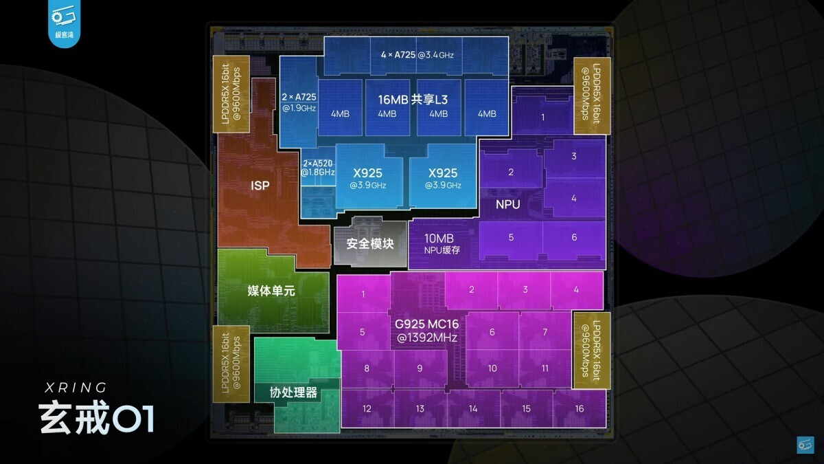
Xiaomi XRING SoCs Possibly Limited to 3 nm, New Restrictions Affecting EDA Software Supply

According to the Financial Times, new restrictions—affecting the supply of Electronic Design Automation (EDA) software suites to Chinese companies—will cause major disruption within the domestic chip design industry. The US government's latest trade amendments are expected to impact Xiaomi and its freshly launched flagship XRING mobile chip family; the first iteration is a compelling first-party effort. Unlike many Chinese tech firms, the popular smartphone specialist can access pretty advanced TSMC node processes. Xiaomi's CEO—Lei Jun—announced his team's 3 nm design during pre-launch preview events.

Days later, closer analysis indicated a selection of TSMC's "N3E" node process. Digital Chat Station—a noted smartphone industry expert—summarized an uncertain future: "under this ban (of EDA tools), XRING chips will not be breaking through a 2 nm barrier, and can only revolve around the (current 'N3E') 3 nm node for a long time. XRING O1 will also be the only time in recent years that it can be on par with current-gen (proprietary) Apple, Qualcomm, and MediaTek mobile chipsets." Crucially, EDA software plays an important role in creating Gate All Around Field Effect Transistor (GAAFET) structures. TSMC's upcoming 2 nm node process is a GAA product. Tom's Hardware believes that several big Chinese tech players, including Huawei, are in the process of developing in-house EDA tools. Not long after unveiling their XRING flagship, Xiaomi outlined an extended Qualcomm chip deal.

ASRock Taking AMD Motherboard and Ryzen CPU Issues Very Seriously

At Computex 2025, ASRock deliberated over the problems that have plagued certain AMD 800-series motherboard models. Fatal combinations—usually affecting popular Ryzen 7 9800X3D gaming CPUs—have been highlighted by sections of the PC hardware community, and (subsequently) press outlets. Months ago, the Taiwanese mainboard manufacturer's Japanese branch took a combative stance (in response to widespread criticism). Following continued failures of Team Red "Granite Ridge" desktop processors on "mid-to-high-end" ASRock mainboards—even in non-3D V-Cache guises—company representatives have interacted with key media conduits, including Tech YES City's Bryan Bilowol. Coinciding with the release of fresh BIOS fixes, long-form video coverage of Q&A sessions have turned up on YouTube.

Company reps have alluded to a warranty replacement scheme, but full details were not disclosed during May-time Computex proceedings. Many critics are still waiting for an official company statement; hopefully addressed to a global audience. In the meantime, one regional office has weighed in with some much-needed outreach: "ASRock Korea takes the recent AMD 800 series motherboard issues experienced by some users very seriously and will follow up with you to protect your trust. ASRock is continuously monitoring the performance and stability of the platform and will provide a firmware update as soon as possible if any issues are identified. In addition, if the system you are using is damaged due to this issue, we will take responsible measures for both the CPU and the motherboard distributed through the official domestic importer, and please submit the case through ASRock Korea's official distributor for diagnosis and processing. ASRock Korea will continue to listen to the voices of our customers and do our best to remain a trusted brand." This message was posted on Quasar Zone; a high-traffic PC hardware forum. A good number of manufacturers have responded to cases raised by members of this South Korean community.

GeForce RTX 5060 8G CYCLONE OC SKU Signals Modern Revival of MSI's CYCLONE Card Series

In 2025, MSI and ASUS seem to be actively engaged in a graphics card product range competition. So far, the Taiwanese manufacturers have launched multiple barebones/budget, mid-range, sub-flagship, and ultra-premium graphics card designs—mostly spanning NVIDIA's GeForce RTX 50-series. At Computex 2025, MSI unveiled a compelling "Retro Line"—by pulling from its back catalog, the veteran hardware firm can deploy extra varieties and flavors for the modern era. Certain PC hardware enthusiasts will have fond memories of MSI's mid-2000s graphics card portfolio—in particular, single-fan model options. VideoCardz has highlighted a pleasing ultra-compact form factor revival; powered by Team Green's GB206 "Blackwell" GPU. At the time of writing, MSI's PR department has not published any promo material.

Instead, a dedicated product page describes a prime "Retro Line" offering: "Cyclone is back. A legacy reborn for a new era—MSI CYCLONE returns with a frosted snow camo design that blends nostalgic charm with modern aesthetics, along with high-efficiency cooling performance." The brand's GeForce RTX 5060 8 GB CYCLONE OC SKU appears to be distinct from a similarly proportioned demonstration unit (presented at Computex, with an integrated display). Unlike their single-fan GeForce RTX 5060 8G INSPIRE ITX card design, MSI's updated CYCLONE model features an open-plan layout. According to an official description: "(our) thermal design concept mirrors the power of a cyclone storm, featuring an advanced aluminium-extruded sunflower radiator, dense fins, and two high-efficiency heat pipes that rapidly dissipate heat from the GPU and surrounding components." Apparently, this diminutive cooler is robust enough to temper an overclocked GPU.

TSMC Confirms No Middle East Expansion and Anticipates Higher Wafer Costs

TSMC has declared that it has no immediate plans to build fabrication plants in the Middle East, reinforcing its strategy to focus on regions where customer demand is strong. Last week's rumors that TSMC might establish a gigafab in the United Arab Emirates have been dismissed by company executives as baseless. CEO CC Wei explained that an expansion into the Gulf does not fit with TSMC's model of locating factories near its largest clients. With ongoing investments in the US, Japan, and Germany, the company aims to serve technology leaders and automotive manufacturers more effectively. Wei added that, without a solid local customer base, building in the Middle East would be impractical. At the same time, TSMC indicated it is reviewing wafer pricing. Fluctuations in the Taiwanese dollar and changing global tariffs were cited as factors under consideration.

According to Wei, long-term agreements could include modest price increases, especially for advanced process nodes, where research and development costs and manufacturing challenges are rising. Looking ahead, TSMC confirmed that the upcoming A14 1.4 nm node wafers are expected to be priced around $45,000 each. This would represent a 50 percent increase over the current 2 nm wafers, which cost about $30,000 apiece. Production of the 1.4 nm node is projected to begin around 2028. Only TSMC's top-tier customers are likely to reserve capacity for this cutting-edge node in its early stages. As demand for advanced semiconductors rises, the company's approach to pricing and geographic focus will be key to maintaining its leadership in the global foundry market.

Acer Predator BiFrost RX 9070 OC 16 GB SKU Hits Retail Two+ Months After Official Unveiling

Acer was late with its contribution of custom RDNA 4 graphics card; introductory press material was issued after the fact, and potential buyers have waited a while for retail stock to reach end destinations. The Taiwanese manufacturer's opening salvo consisted of premium "Predator BiFrost" and sub-flagship "Nitro" overclocked Radeon RX 9070 XT models, but non-XT options did not launch at the same time. This morning, VideoCardz noted the availability of Predator BiFrost RX 9070 OC 16 GB cards in Japan. The company's regional office has opened its direct-to-customer order book; to the tune of 128,800 yen (including sales tax) per unit—converting to roughly ~$902 (USD).

Unlike XT equivalents, Acer's Predator BiFrost OC and Nitro OC RX 9070 models feature two 8-pin power connectors (instead of three units). Currently, the Geizhals/Skinflint price aggregator denotes stock—of both SKUs—being present at e-tailers in Germany and Austria. According to comparisons, the best Predator BiFrost RX 9070 OC deal comes in at €709 (inc. VAT), at GALAXUS. PLAYOX and Office-Partner.de offer the lowest Nitro RX 9070 OC price tags: €669 (inc. VAT), plus €4.99 processing fees. Acer has not publicly disclosed the reasons behind subsequent sluggish launches of its RDNA 4 portfolio. Curiously enough, Yeston—best known for dealing in eccentric card designs—foresaw a post-April stabilization of Radeon RX 9070 series shipments.

ASUS TUF Gaming Talks About Hatsune Miku Crossover Collection

The undisputed number one princess in the world, Hatsune Miku, has conquered hearts the world over. But her blue hair and blue tie don't have to stay hidden in your WiFi. With the TUF Gaming x Hatsune Miku collection, the world's most famous vocaloid can sing along with you through your gaming peripherals. Special Hatsune Miku editions of the TUF Gaming K3 Gen II gaming keyboard, TUF Gaming H1 Gen II gaming mouse, TUF Gaming Mini Wireless mouse, and TUF Gaming P1 gaming mouse pad bring a cybernetic fusion of Miku's signature blue-green and pink color scheme along with the mechanical-armor aesthetics of TUF Gaming.

Durable, compact, and stylish: The TUF Gaming K3 Gen II Hatsune Miku Edition keyboard
Finished in the Hatsune Miku color scheme, the TUF Gaming K3 Gen II Hatsune Miku Edition gaming keyboard makes a stunning first impression. Miku-themed touches abound across its surfaces, including specialized keycaps for the Enter keys, spacebar, Esc key, and more. Per-key RGB LED illumination with up to 16.8 million colors, customizable through ASUS Aura Sync, lets you personalize the look of the board. But can you truly say from the bottom of your heart that Miku is adorable if you stray too far from her signature colors?

PowerColor Readying Spectral White Radeon RX 9060 XT Hellhound & Reaper SKUs

PowerColor introduced four custom Radeon RX 9060 XT options during Computex 2025; consisting of standard black mid-range Hellhound and entry-level Reaper models. The dark 16 GB and 8 GB launch lineup will be joined by Spectral White sibling in the near future. The manufacturer's China website was updated with three pale alternatives at some point last week. Currently, only the Radeon RX 9060 XT 16 GB Hellhound Spectral White SKU has made tracks over to the Taiwanese brand's global web presence. The company's Navi 44 XT GPU-based portfolio is not expected to welcome premium-tier Red Devil entries, so the current collection—of seven distinct offerings—will suffice.

Curiously, the two Reaper models seem to differ in terms of clock speeds. As noted by VideoCardz, this specification disparity reflects a recently reported difference between Yeston's Radeon RX 9060 XT 16 GB and 8 GB GAEA SKUs. Almost akin to patterns exhibited by the Chinese AIB's baseline MSRP conformant products, the PowerColor Reaper 16 GB card seems to boast greater game and boost clock digits when compared to its 8 GB sibling: +90 MHz and 100 MHz (respectively). At first, Yeston's GAEA spec charts were believed to contain placeholder info or anomalous data. The appearances of comparable PowerColor examples indicate an advantageous position for certain 16 GB GDDR6 VRAM-equipped models.

PowerColor Radeon AI PRO R9700 Card Design Reminiscent of AMD's Reference Renders

Last week, AMD introduced its Radeon AI PRO R9700 32 GB professional graphics card—representing the RDNA 4 generation's first foray into non-gaming territories. The TechPowerUp team encountered board partner variants on the showroom floor, with GIGABYTE and ASRock exhibiting samples with blower-style cooling solutions. At the time, Team Red's reference design was only visible in promotional/artistic renders. According to the company's official product page, this particular model is "not available for purchase." AMD made similar claims during the early days of—related Navi 48 GPU-based—Radeon RX 9070 XT and RX 9070 cards. Months later, Chinese hardware enthusiasts picked up physical "Made-By-AMD" (MBA) examples via murky second hand market channels.

At some point this week, PowerColor's web presences were updated with a semi-familiar sight: an almost direct interpretation of the AMD Radeon AI PRO R9700 reference card. The Taiwanese AIB has removed "AI" and "PRO R9700" text from their variant's shroud design, and applied a customary "PowerColor" logo and symbol sticker onto the lone blower fan's face. VideoCardz believes that pre-announcement renders and specification leaks had caused confusion across insider networks—hence the emergence of "Radeon RX 9070 XT(X) 32 GB" rumors, within the first quarter of 2025. PowerColor did not showcase its pro-grade at the recently concluded Computex trade event—instead, company representatives were tasked with hyping up incoming custom Radeon RX 9060 XT gaming cards, and a mysterious "REVA" prototype. At the time of writing, PowerColor has not issued any Radeon AI PRO R9700-related press material. AMD and manufacturing partners are expected to launch finalized products in July.
Return to Keyword Browsing
Nov 11th, 2026 04:12 CST change timezone

New Forum Posts

Popular Reviews

TPU on YouTube

Controversial News Posts