News Posts matching #Taiwan

Return to Keyword Browsing

Amkor to Significantly Boost Arizona Packaging Capacity for Intel and TSMC

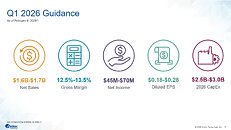
Amkor is preparing to greatly expand its Arizona-based operations, and the company will boost its spending not by a few percent, but by several multiples. The company is planning to triple its capital expenditures next year, with a dramatic increase from roughly $900 million in 2025 to as much as $3 billion in 2026, betting on massive demand from Intel and TSMC packaging technologies. This includes working with Intel and TSMC to enable their most advanced technologies like EMIB and CoWoS, all of which come in various form factors. We previously reported that Intel partnered with its long-time OSAT partner Amkor to take additional EMIB capacity that Intel's customers are interested in, in Incheon, South Korea.

However, as Amkor expands its facilities in Arizona, Intel will also collaborate with Amkor to deliver advanced EMIB packaging types on United States soil. While TSMC has been a primary choice for many high-density assemblies, growing interest in Intel's EMIB and Foveros options has led partners like MediaTek, Google, Qualcomm, and Tesla to consider alternatives. Interestingly, Amkor will also offload some of the CoWoS packaging work from TSMC by creating CoWoS packages on U.S. soil, instead of sending these chips back to TSMC's Taiwan fabs to finish production. Both CoWoS and EMIB/Foveros offer a list of benefits, making them highly sought-after packaging technologies for companies seeking to extract maximum performance from their chips. Amkor plans to be at the center of that supply chain and help Intel and TSMC handle more customers.

MSI GeForce RTX 5090 Lightning Z GPU Listed at $5,200 in Taiwan

MSI's most powerful GPU—the GeForce RTX 5090 Lightning Z—will come with an extreme price tag to match, as the company has listed its GPU for NT$165,000, which works out to about $5,200. The company noted this pricing in a 24-hour giveaway scheduled to begin on Monday, February 9, at 10:00 AM Taiwanese time, lasting until Tuesday, February 10. The listing has revealed that the card we previewed at the 2026 International CES show is not only a premium design but also a premium-priced product, as the supply is limited to only 1,300 samples. MSI advertises a factory boost clock of 2,730 MHz and an "Extreme Performance" OC profile of 2,775 MHz. Additionally, the GPU is capable of reaching 3,742 MHz, which is the fastest LN2 GeForce RTX 5090 GPU ever.

The MSI GeForce RTX 5090 Lightning Z will come with an 800 W power limit out of the box, while the "Extreme" power preset mode gives it a 1000 W power envelope on the 360 mm AIO water cooling. The extensive engineering involved in the PCB design along with a 40-phase VRM allows the GPU to sustain multi-kilowatt loads. The card uses 28 Gbps Samsung GDDR7 memory, which can be overclocked to 36 Gbps on LN2. Additionally, only LN2 is capable of taming the XOC BIOS, which comes with 2.5 kW of power load and will require extensive PCB modifications. For a product that costs $5,200, only extreme overclockers would dare to modify the card. For the rest of us mere mortals, MSI recommends a power supply with a capacity of 1600 W, providing ample room for basic overclocking without ruining the card.

Silicon Motion Announces Results for the Fourth Quarter and Year Ended December 31, 2025

Silicon Motion Technology Corporation (NasdaqGS: SIMO) ("Silicon Motion," the "Company," "we" or similar terms) today announced its financial results for the fourth quarter and year ended December 31, 2025. For the fourth quarter of 2025, net sales (GAAP) increased sequentially to $278.5 million from $242.0 million in the third quarter of 2025. Net income (GAAP) also increased sequentially to $47.7 million, or $1.41 per diluted American depositary share ("ADS") (GAAP), from net income (GAAP) of $39.1 million, or $1.16 per diluted ADS (GAAP), in the third quarter of 2025.

For the fourth quarter of 2025, net income (non-GAAP) increased sequentially to $42.7 million, or $1.26 per diluted ADS (non-GAAP), from net income (non-GAAP) of $33.8 million, or $1.00 per diluted ADS (non-GAAP), in the third quarter of 2025. All financial numbers are in U.S. dollars unless otherwise noted.

NVIDIA's Taiwan HQ Plans Approved by Ministry of Economic Affairs

The Ministry of Economic Affairs (MOEA) in Taiwan has approved NVIDIA's application for its planned local headquarters in the Beitou-Shilin Technology Park. The investment of NT$3.3 billion—or just over US$105 million—was approved a day ahead of Jensen Huang arriving in Taiwan to celebrate the Lunar New Year at a traditional weiya banquet alongside NVIDIA staff. According to CNA, the local subsidiary will be named NVIDIA Iconic Taiwan Co. Various NVIDIA partners are expected to attend the weiya as well, although the Taiwan media hasn't reported on any specific companies as yet.

The plot where the new headquarters will be built was originally meant to house a local insurance company, but as the insurance company had left the plot—which it won in a public tender—empty since 2021, the Taipei City Government negotiated a termination of the contract and NVIDIA will now be taking over the plot. The contract with NVIDIA is expected to be signed ahead of the Lunar New Year which starts on the week of the 16th of February. NVIDIA has revised its investment multiple times and only a couple of months ago, it was reported that the company was going to invest NT$1 billion, or US$32 million. It's unclear why the investment has trebled since then.

ASUS Prepping Motherboard BIOS Updates for Core Ultra 200K+ "ARL-S R" CPUs

Intel did not introduce its oft-leaked "Arrow Lake Refresh" desktop and laptop CPU ranges at CES 2026, despite plenty of pre-event activity suggesting a near future arrival at retail. Almost two weeks after the conclusion of new product promotional activities in Las Vegas, ASUS has just started to hype up its own "in advance" preparations for Team Blue's inevitable release of "ARL-S Refresh" desktop chips. A few hours ago, the Taiwanese hardware manufacturer's main social media account proudly declared: "ready for the future of Intel! ASUS W880, Z890, Q870, B860 & H810 motherboards are BIOS READY—rolling out in late January." Leaked "Core Ultra 200 Plus" nomenclature suggests that Intel has kept its slightly upgraded designs within the Core Ultra Series 2 generation. Previously, their refreshment of "Raptor Lake" was deemed worthy of becoming a new processor generation: 14th Gen Core.

Curiously, today's ASUS announcement labels the latest mid-gen refresh as next generation: "all set for Intel Arrow Lake Refresh! Upgrade smoothly. Next-gen power is coming!" Gaming CPU market segment trackers believe that the "Plus/+" designation will only turn up on three new SKUs: Core Ultra 9 290K Plus, Core Ultra 9 270K Plus, and Core Ultra 5 250K Plus. This seemingly sparse lineup is expected to keep Team Blue's LGA 1851 platform propped up for a little bit longer, until the successive and truly next-gen "Nova Lake-S" desktop family rolls up with its matching LGA 1954 socket. About a week ago, Golden Pig Upgrade predicted that Intel would launch Ultra 200 Plus desktop and laptop/notebook (HX) products within a March/April window. Coinciding with ASUS readying BIOS updates for 800-series motherboard later this month, Intel and its hardware partners will be unleashing Core Ultra 300 "Panther Lake-H" mobile processors.

Jensen Huang Believes that NVIDIA is TSMC's Premiere Customer - Foundry Reportedly Deprioritizes Apple

A recent Jensen Huang declaration and fresh chip production industry rumors have coalesced nigh simultaneously. During a sitdown with Jodi Shelton—on her "A Bit Personal with..." podcast—the Team Green boss made a lofty claim when asked about his confident approach when conducting business: "well, you know, it's rough to know everything—I'm just kidding...By the way, Morris (Chang) will be happy to know (that) NVIDIA is TSMC's largest customer now." Almost perfectly timed industry whispers have emerged—within the past day or two—suggesting Taiwan's leading foundry service adjusting its supply relationship with Apple. Previous to current tremors, the Cupertino-headquartered giant has reportedly enjoyed priority access to cutting-edge node processes. Yesterday morning, the "Fixed-focus Digital Cameras" Weibo account let slip about a speculated trip, stateside, made by TSMC's Che-Chia Wei.

The short blog entry alleged that the TSMC CEO visited: "Apple HQ (in order) to demand the largest price increase in recent years, and Apple may no longer enjoy priority production capacity. TSMC's largest customer is now NVIDIA, accounting for nearly 13% of total revenue." The two fabless rivals seemingly want unobstructed access to 2 nm wafer production lines, but Team Green has supposedly got the edge here—very likely driven by successes in the AI enterprise field. According to fairly fresh inside track information, Apple has secured around half of TSMC's 2 nm manufacturing capacity—linked to forthcoming A20 and A20 Pro smartphone chipsets. In terms of proprietary AI server-grade designs, the house of Mac and iPhone is reported to be working on an inference-only "Baltra" GPU project. Industry moles have mentioned the selection of a TSMC 3 nm node (N3E or N3P) for this far-off-from-launch prospect.

Samsung's Texas Fab Reportedly Attracting Major Customer Interest as AI Boom Continues

A report put together by Deutsche Bank analysts has mentioned an ongoing supply-demand imbalance within the semiconductor market. According to Jukan's summary of the financial institute's findings, TSMC's "share of the advanced-node foundry market" could fall from an impressive 95% level, down to a mere 90% in the coming years. The industry-leading chipmaker continues to enjoy a prime position, but its international operation footprint seemingly cannot keep up with requests—mainly from fabless customers—during the ongoing AI hardware boom. Deutsche Bank believes that the Taiwanese foundry business has an order backlog extending way into 2027, with many clients requiring 3 nm wafer products. TSMC reportedly aims to get 3 nm node production lines pumping out around 190,000 wafers per month, by the end of this year. Even if this major target is met, demand is expected to outweigh supply. AI chip production-centric bottlenecks—mostly involving CoWoS packaging—have been dealt with in the recent past, but industry observers posit that VIP customers are considering alternate providers.

Allegedly, the next best options are the Samsung and Intel Foundries, despite rumors of teething problems—both companies will very likely welcome new requests. In modern times, many of Samsung's big clients have switched over to TSMC, due to (the former's) supposedly troubled development of more advanced nodes. Deutsche Bank analysts have outlined a "big six" group of key customers: AMD, Apple, Broadcom, MediaTek, NVIDIA, and Qualcomm. The fabless firms could be pursuing alternate "production capacity" avenues, with Samsung's 2 nm (SF2) and 4 nm node process lines being of particular interest. Like TSMC, the South Korea megacorp's state-of-the-art fabrication sites and staff expertise are concentrated in home territories. A surprise prediction has highlighted Samsung's main North American foundry—the Deutsche Bank report pinpointed a very specific location: "for customers seeking alternative supply, Samsung's Taylor fab is more likely to become the first destination." In addition, analysts think that the big six will select Samsung's Texas-based foundry over Intel's best native site (perhaps dealing in 18A).

NVIDIA's GPU Memory Bundles Cost Less Than AMD's, Note AIB Partners

Taiwanese media outlet Benchlife has reportedly obtained information about the pricing of AMD and NVIDIA GPU and memory bundles shipped to their respective add-in-board partners. According to their findings, both AMD and NVIDIA have increased the prices of GDDR6 and GDDR7 memory to reflect the current industry-wide DRAM shortage. However, the report highlights that NVIDIA's pricing for GDDR6 and GDDR7 memory is significantly lower than AMD's. As AMD and NVIDIA bundle their GPU dies with GDDR6/GDDR7 memory, they can set the pricing of these bundles based on several factors. These factors include the cost at which they acquire the DRAM and the desired profit margin for the GPU dies. Typically, the memory is paired with the GPU die, which also influences the final pricing strategy.
BenchlifeOn January 16th, NVIDIA officially notified its AIC partners that all bundled GDDR6 and GDDR7 memory packages are now increasing in price. We have been informed of the price increase through familiar AIC partners, but we won't specify the exact price here. What we can say is that NVIDIA's new prices are still lower than those announced by AMD to its AIB partners.

First Shipments of NVIDIA "Vera Rubin" AI Servers Expected Around Late Summer

Last week, Quanta Computer's Mike Yang let slip details about the eventual arrival of NVIDIA "Vera Rubin" AI server hardware. The executive vice president/general manager mentioned potential first shipments—heading in the direction of hyperscalers—occurring by August of this year. According to Taiwan's Commercial Times, this prediction was disclosed during an official celebratory company event (on January 15). Additionally, the Quanta boss does not expect a widespread deployment at that point in time, and (consequently) significant revenue generated by sales of new "Vera Rubin" equipment. According to the exec's statements, "most" customers are already running operations based on current-gen "Grace Blackwell" GB200 and GB300, but Yang believes that common architectural traits will make transitions—onto the next-gen platform—much easier than before.

Industry observers have highlighted possible issues of moving from the "Grace Blackwell" chiplet-based design to the advanced packaging of "Vera Rubin." During CES, NVIDIA announced that full production of server-grade "Vera" CPUs and "Rubin" GPUs had kicked off. This Q1 2026 initiation has happened well ahead of a previous "by H2 2026" mass manufacturing goal. Team Green's forthcoming "Vera Rubin" NVL72 SuperCluster is classed as a premier rack-scale system. A larger "NVL144" variant was previewed last year, but this CPX platform seems to be further out from release. According to a mid-October report, an involved manufacturing partner was weighing up a loose "2026 volume production" window.

MSI's Ryzen Z2 Extreme-powered Claw A8 Handheld Finally Lands at US Retail Outlets

In the run-up to Christmas, MSI seemed to be readying its Claw A8 handheld gaming PC for imminent launch in North America. At the time, a handful of fresh listings—minus price and release date info—were noticed by web detectives. Over a month later, the US-specific "BZ2EM-070US" model is currently in stock at MSI's regional official store, and ready for pre-ordering chez ExcaliberPC. The latter is already offering a special discount—$1099 instead of the usual $1149. Despite being the first North American online shops to list MSI's Polar Tempest-finished portable device, Newegg and B&H Photo do not have any stock—at the time of writing. MSI's latest geographically staggered gaming handheld roll-out is a bit of a head scratcher, given that their Ryzen Z2 Extreme APU-powered Claw A8 debuted in Asia almost half a year ago.

Demonstration units were present at the company's CES 2026 booth, with representatives informing visitors about the Team Red-based system "officially coming to North America," albeit only in "Tempest White." Other territories have been granted access to a "Neon Green" version. During a hands-on session with Claw A8 samples in Las Vegas, The Outer Haven was informed about circumstances that have affected the hardware's westward journey: "(MSI's rep) explained that the tariffs placed against China made it difficult to release the device in North America under the original production setup. To make the US release possible, MSI adjusted where parts were sourced and where assembly took place, shifting manufacturing from China to facilities in Taiwan and Korea." The Claw A8 BZ2EM-070US model (24 GB LPDDR5x + 1 TB SSD) faces plenty of competition in early 2026, and the rise of "Panther Lake-H"-powered next-gen handhelds later on in the year.

Micron to Buy Fab From PSMC in Taiwan to Increase DRAM Output

Micron has signed a letter of intent with Taiwanese Powerchip Semiconductor Manufacturing Corporation (PSMC) to buy its P5 fab in Tongluo in Central Taiwan. Micron and PSMC have agreed on a cash price of US$1.8 billion for the fab, which is PSMC's most recent 12-inch fab and should allow Micron to add additional 1x nm DRAM production capacity. The two companies are expecting the transaction to close by the second quarter of this year, but it doesn't mean that Micron will take over the facility from day one. Instead, Micron isn't expecting the fab to "contribute to meaningful DRAM wafer output" until the second half of 2027.

PSMC doesn't have its own 1x nm DRAM production today, as the company is still developing its own nodes, which could be part of the reason for the delayed "meaningful" output for Micron. That means that with the current equipment in place, Micron will end up with 2x nm DRAM to start with, suggesting it's DDR4 that's being produced at the fab today. According to TrendForce, the fab should be able to contribute as much as 10 percent of Micron's total DRAM output in 2027, which is not an insignificant amount. TrendForce also noted that PSMC is expecting to get a 1x nm (1Y or 1Z) DRAM license for its other fabs, to help it produce higher-density DRAM in the near future at its other fabs.

TSMC Expecting to Start 3 nm Production in Arizona in 2H 2027

Almost two years after it started mass production of 2 nm chips at Fab 22 in Kaohsiung, Taiwan, TSMC is expecting to kick off 3 nm production in what will be its second fab in Arizona, USA, according to a comment by its Chairman C.C. Wei to the Taiwan media. The new fab was originally not planned to go online until 2028, but it has now been moved forward to the second half of 2027 and TSMC is also planning a fourth fab and an advanced chip assembly plant on the same plot. TSMC has pledged to invest a further US$100 billion to build a further three fabs in Arizona, alongside two IC assembly plants and an R&D centre, with 2 nm production currently slated for 2029.

The company has acquired additional land in Arizona to be able to expand its complex in Arizona into what Wei called a "megafab cluster" to be able to meet their customers' demands. What is less clear is where TSMC is going to find the factory workers, as the company has already been having issues with labour in the US. Wei also mentioned that construction of its second fab in Kumamoto, Japan has started construction and that the construction of its fab in Dresden, Germany is proceeding according to plans. At the same time, TSMC is planning additional fabs in Hsinchu and Kaohsiung that will be building chips on its 2 nm node or more advanced nodes.

ASRock Website Updated with Radeon RX 9070 XT Taichi White OC Model Page

In the run-up to Christmas, ASRock unveiled a pale spin-off of its readily available Radeon RX 9070 XT Taichi OC graphics card model. As of this week, gaming graphics card sleuths have noticed that the Taiwanese manufacturer has published a dedicated product page. A "RX9070XT TCW 16GO" code, detailed specifications, various product and feature set descriptions, and plenty of images are on full display on ASRock's main web presence. TechPowerUp's CES 2026 ground team did not spot a white Taichi demonstration sample during a past week ASRock suite visit. An official pre-event PR piece implied some form of early January trade show concurrent introduction.

Their latest update of the custom RDNA 4-based flagship manages to implement a new "LCD Information Center" feature—simply a dinky side-mounted 2-inch color LCD screen that can broadcast key diagnostic data and animations. Early promotional renders indicated that ASRock had bunged on a longer strip of ARGB lighting across the white Taichi variant's top-side. A full selection of shots show off this new zone, complete with an expansion of this Taichi generation's gear-themed aesthetic. The added extras have tacked on a little bit of extra weight (+67 g), relative to the metallically-dressed standard Taichi model—ASRock's specification sheet lists a slightly heavier net weight measurement of 1621 grams. The white RX 9070 XT Taichi OC variant is still a three-slot thick behemoth, with an additional 6 mm tacked onto its depth dimension (according to official specs).

ASRock Presents New DeskSlim, DeskMini, & Box PC Systems at CES 2026

Earlier today, ASRock granted TechPowerUp access to its mostly new product laden Las Vegas hotel suite, where several brand-new mini PC systems immediately drew the eye. The Taiwanese manufacturer's DeskSlim B760 is already a somewhat known property, but over a month later, it is encouraging to examine a demonstration unit in-person. ASRock's demo example was already opened up when TPU turned up on the scene; clearly showing Intel hardware-based innards. Team Blue's reference Arc Pro B50 "Battlemage" workstation-grade graphics card is dinky enough to fit inside the DeskSlim B760 model's ultra-compact 4.9-liter chassis. Also, a Laminar RH-style air cooler was crammed into the tight interior space—tasked with cooling up to Intel 14th Gen Core CPUs. A nearby product placard mentions that the AMD-based DeskSlim X600 variant is also on the way to launch.

Bitspower Shows Off CPU Cooler Prototype with Multiple Mounted LCD Screens

Bitspower has a curious demo setup tucked in a corner of its Las Vegas suite. A cuboid CPU cooler—featuring three LCD screens—sits atop a dummy ATX-shaped motherboard. PC builders have become accustomed to the presence of single screens on various types of modern central processor cooling solutions. In stark contrast, Bitspower has opted into prepping an unusual triple-panel array that is hooked up to a nearby tablet. A proprietary application allows users to select picture, GIF or video content and adjust displayed diagnostic information. The tablet was also put in charge of controlling ARGB lighting systems present on connected fans.

Considering the size of the block mounted onto the plastic board, initial inspectors would conclude that Bitspower's engineering team had created some sort of air-cooled tower. The absence of fans and a dense matrix fin array indicates an alternative method; perhaps not passive. TechPowerUp lifted up the demonstration block and found part of a liquid cooling pump fixed onto the pretend CPU socket. Most of Bitspower's prototype seems to be made of dark gray plastic, and simply serves as a set of surfaces to affix LCD screens onto. Amusingly, the dummy mainboard sports four mock sticks of RAM—a wishful provision given current market conditions!

MediaTek Reportedly Prioritizing Development of AI ASICs Over Mobile Chips

MediaTek's growing partnership with Google has reportedly prompted a shift in development priorities; industry insiders propose an ongoing "realignment" of internal resources. The alleged formation of a dedicated ASIC division seems to be draining staff away from the more visible Dimensity mobile chip projects—by previous announcements, a very important aspect of the Taiwanese fabless semiconductor firm's business. Going back to March 2025, MediaTek and Google partnered up on the making of a seventh-gen "Ironwood" Tensor Processing Unit (TPU) design. Later in the year, it emerged that MediaTek engineers were assisting on Google's even more futuristic "Zebrafish" TPUv8x project.

Industry analysts posit that the demands of formulating Google's complex/intricate 3 nm TPU v7 design has taken precedence within MediaTek operations; prompting the rumored formation of a full-fledged ASIC department. Another key factor seems to be a tight timeline that leads to significant volume orders of Google TPUs. According to a Commercial Times Taiwan news article, mass production is expected to start within the third quarter of 2026. Future targets include five million units pumped out by 2027, followed by an ambitious seven million unit goal in 2028. Similarly, Broadcom is "actively preparing production capacity" for its Google TPU collaboration. Local reportage points out that Rick Tsai—MediaTek's Vice Chairman and CEO—anticipates pleasing financial results related to his team's "first ASIC project." Smooth progress in 2026 could lead to an approximate $1 billion revenue contribution, with forecasts of several billion dollars in 2027. Another major earner could emerge from a speculated deal with Meta—MediaTek's second ASIC project is said to be based on an unnamed 2 nm node process.

TSMC Kicks Off 2 nm Mass Production

TSMC has announced that it has started 2 nm mass production in Fab 22 which is located in the southern city of Kaohsiung in Taiwan. This is TSMC's first fab this far south in Taiwan and it's the first phase of as many as five that will be at this location. The fab is using 300 mm wafers and TSMC's first-generation nanosheet transistor technology on the N2 node. TSMC has already stated that the N2 node is offering a full node jump in terms of performance and power benefits, although the company is comparing the N2 node to its second generation N3E node, not the original N3 node, suggesting that the N2 node is slightly better than a regular full node improvement for TSMC.

The N2 node also includes some new additions that TSMC claims will further boost performance, in the shape of a low-resistance redistribution layer (RDL) and super high-performance metal-insulator-metal (MiM) capacitors. Time will tell how these advancements play out in real world products, once we find out which customers are first out with chips built on the N2 node. The N2 node is said to offer a 10 to 15 percent performance increase at the same power consumption or a 25 to 30 percent reduction in power at the same performance, compared to the N3E node, as well as a transistor density increase of around 15 percent.

Maxsun Engineers Cram Four DIMM Slots Onto New "MS-PC Farm B860I" Mini-ITX Model

On Wednesday (December 17), Maxsun presented its brand-new PC Farm motherboard series at this year's Shunwang Technology and Intel Cloud Business Summit. The Taiwanese computer hardware specialist introduced three options (in slide form only): MS-PC Farm B760I, MS-PC Farm H770I D5 V2, and MS-PC Farm B860I. The latter SKU has attracted the most attention, due to it featuring: "four DIMM slots (that support) up to 256 GB of (DDR5) memory." Maxsun's PR department reckons that this configuration will be ready to "meet high-load computing demands." A single low resolution promo shot shows off a largely black Mini-ITX board design, with a third of its real estate occupied by four DIMM slots. Initial press analysis proposes that Maxsun's upcoming product could be the first of its kind; a tiny consumer-grade board that can accommodate four sticks of DDR5 RAM.

Normally, compact PC enthusiasts—desiring 4-slot setups—have compromised with selections of larger microATX parts. Maxsun's MS-PC Farm flagship model builds on "existing airflow optimization and IPMI management capabilities." The company's preview material outlines support on the MCIO interface for high-speed PCIe 5.0 expansion. Also, the MS-PC Farm B860I is capable of "forced BIOS flashing." An intelligent fault diagnosis system is advertised as being able to accurately locate: "problems with various IC components on the motherboard for rapid troubleshooting and recovery, ensuring continuous and stable system operation." A full specification sheet was not released during a mid-week preview event, but the presence of an Intel B860 chipset and LGA 1851 socket pave the way for hosting of current-gen Core Ultra 200S "Arrow Lake" processors.

TSMC USA's Access to Cutting-edge Nodes Could be Stymied by Taiwanese Regulations

According to recent reports, TSMC leadership is expediting a major next phase at the Arizona campus—a second fabrication facility could come online by 2027, with a move into mass production of 3 nm (N3) wafers. A fresh news article—published by CNA Taiwan—signals an uncertain technological roadmap for the leading foundry service's North American operations. Taiwanese regulators have reportedly questioned TSMC's commitment to a long-term "N-2" rule. Under strict guidelines, the nation's premier chipmaker is not allowed to narrow a two generation-wide gap between domestic and offshore foundry capabilities. Presently, the Arizona Fab 21 Phase 1 site—at best—can pump out 4 nm (N4) products. Additionally, it produces more mature 5 nm (N5) wafers.

Given the current global political climate, TSMC's executive team could have a tough time satisfying demands from both sides of the Pacific. CNA's news piece highlighted observations made by Lin Fa-cheng, the Deputy Minister of Taiwan's National Science and Technology Council (NSTC). According to that report, Fa-cheng believes that TSMC will continue to adhere to the "N-2" policy, due to the vast majority of company R&D expertise being concentrated domestically—once native development moves onto the creation of truly cutting-edge 1.2 nm and 1.4 nm technologies, their 1.6 nm-class process (A16) knowledge can be shared with overseas facilities. Almost a month ago, insiders posited that TSMC was planning another expansion of its home turf footprint—a speculated $28 billion investment could lead to the construction of three 2 nm specialist fabs.

ASUS DUAL GeForce RTX 5060 Ti & 5060-series Slimmed Down with "2.1-slot" EVO Models

ASUS has expanded its DUAL graphics card family with a smattering of lower-end models—based on NVIDIA's GB206 "Blackwell" GPU—that offer a slimmer profile. Brand-new listings, added in a low-key manner—are tagged with "EVO" designations. As highlighted by Vortez, the DUAL EVO design comes in at "2.1-slot" thickness (42 mm). This slight shrinkage—mostly in one dimension: width—distinguishes new entries from standard DUAL options. The latter examples exist as 2.5-slot thick (50 mm) offerings. There are negligible differences—between twin axial tech-fan cooled EVO and non-EVO SKUs—in terms of card length and height.

At a glance, ASUS has only introduced this slimmer shroud design across overclocked (OC) edition and non-overclocked GeForce RTX 5060 Ti 16 GB and RTX 5060 8 GB models. Confusingly, this generation's EVO aesthetic actually debuted mid-way through 2025, under the guise of vanilla DUAL GeForce RTX 5050 graphics card options—all truly 2.0-slot (40 mm) thick. This brand-new wave of cards has lead to an adjusted placement of single 8-pin power connectors—DUAL GeForce RTX 5060 Ti and RTX 5060 EVO designs have this aspect positioned closer to their I/O brackets. The TechPowerUp readership can familiarize itself with a myriad of DUAL EVO and DUAL options present within the site's well-maintained GPU database. Fresh entries popped up before the publication of this news piece.

MSI Claw A8 Nearing Retail Release in USA, Approx. 4 - 5 Months After Launch in Asia

MSI's AMD APU-powered Claw A8 handheld gaming PC seems to be heading to North American shores. Over the past weekend, web sleuths noticed Newegg and B&H Photo Video listings. At the time of writing, a pre-release price tag—$1149—is attached to the territory specific "BZ2EM-070US" SKU. Reflecting similar past practices, MSI has staggered the rollout of its latest Windows 11-based portable gaming system. The Taiwanese manufacturer has tended to favor Asian territories when distributing the first waves of Claw hardware—notably, the current-gen A8 debuted in China (and nearby) around "late July/early August."

Unlike most of the competition, MSI opted into using Intel APUs across first and second-generation Claw platforms. Even in Core Ultra 7 form, Team Blue's "Meteor Lake" chipsets trailed behind competing AMD-centric hardware. MSI's second wave handheld PCs—Claw 8 AI+ and Claw 7 AI+—were driven by Intel's Core Ultra 7 258V APU. This "Lunar Lake" mobile processor currently competes with Team Red's AMD Ryzen Z2 Extreme SoC, as tracked/observed by Golden Pig Upgrade. Around mid-May, we picked up on whispers of the MSI Claw family diversifying into the AMD APU realm. A couple of months later, the Ryzen Z2 Extreme-powered Claw A8 started to trickle out at retail. Eventually reaching UK stores by September; priced at £849 (~$1135 USD)—available in Polar Tempest (white) or Neon Green finishes. Presently, only the white 1 TB + 24 GB LPDDR5X model is listed by Newegg and B&H.

Acer Launches White Edition Predator BiFrost Radeon RX 9070 XT/9070 Cards

Acer introduced its opening salvo of Radeon RX 9070 XT 16 GB and RX 9070 non-XT 16 GB custom card designs back in March, almost alongside competing options produced by other AMD board partners. Oddly, the Taiwanese computer hardware manufacturer did not end up launching Navi 48 GPU-based products during that period—months later, retail stock started appearing in Japan. Fast-forward to the end of 2025, and Acer seems to be catching up with other AIBs, yet again. Last Friday (December 12), a Japanese press release signalled the arrival of White Edition Predator BiFrost options at retail outlets. The flagship spin-off SKU is available immediately, at 138,800 yen (tax included), converting to ~$896 USD.

A weekend investigation—prompted by GDM/hermitage akihabara's PR release—produced evidence of pale Predator BiFrost Radeon RX 9070 XT OC and RX 9070 OC stock reaching Europe. VideoCardz happened upon highly-detailed entries on the Geizhals price aggregation engine. In Germany, Acer's best RDNA 4 gaming card—now dressed in white—is (appropriately) cheapest at the "NBB - notebooksbilliger" Ebay store. An active voucher promo brings total cost of ownership down to €613.81 (~$722 USD). Alternatively, NBB and Nullprozentshop offer the joint-lowest non-XT White Edition listings: €539.00 (~$634 USD). Product renders show familiar packaging; already present on boxed standard black models. Oddly, the non-XT promotional shots show the deployment of three 8-pin power connectors (instead of the standard two). Normally this triple provision is reserved for top-level XT options, so Acer's graphics department could be using a generic image set for both overclocked models.

ASUS Hints About Dual Battery Config in Next-gen Zenbook Duo Model

Earlier today, the global ASUS social media account kicked off a marketing campaign for a futuristic Zenbook DUO design. A brief but slick trailer drives two key points into viewer's retinas: "Next Level Durability" and "Next Level Power That Lasts." The 22-second-long teaser video focuses on sturdy-looking hinge systems, and then a glowing pair of power cells. The CGI cutaway shows a depiction of batteries being stashed inside both halves of the device. According to quick Wccftech research, Lenovo's ThinkPad T580 15" model seems to contain a similar setup, albeit minus dual-displays—granting an advertised/claimed 27-hour-long battery life. ASUS confirms that the next-gen Zenbook DUO high-end notebook model will be unveiled at CES 2026. Specifically, during a January 6 special online event/livestream.

Current-gen Zenbook DUO (UX8406) options are fitted with two "full-size" 14-inch 3K 120 Hz OLED touchscreens. The most potent variant is driven by Intel's Core Ultra 9 285H APU. This flagship mobile processor—sitting atop the "Arrow Lake-H" series—sports an Arc Graphics 140T (Xe-LPG+) iGPU. The 2026 Zenbook DUO could be treated with a next-gen hardware upgrade—potentially "Panther Lake-H." Recent leaks signal an imminent introduction of Team Blue's next-wave flagship chip: Core Ultra X9 388H. A very capable 12-Xe3 core iGPU will have an easier time running twin ultra-resolution/high-refresh displays. The short Zenbook DUO 2026 teaser provides a blurry look at a revised detachable keyboard design. When compared to current accessories, a larger trackpad seems to be present, along with recessed keys, and a slimmer profile.

TSMC Reportedly Weighing Up Upgrade to N4 & N5 Nodes at Phase 2 Japanese Fab

Semiconductor industry insiders reckon that TSMC leadership has revised its production strategies for a Japan-based fabrication site. The Taiwanese foundry business owns a majority stake in Japan Advanced Semiconductor Manufacturing (JASM). This partnership lead to a "Fab 23 phase 1" plant coming online a year ago, in the Kumamoto Prefecture. This factory is tasked with producing past-gen-sized wafers; at best on a 12 nm process node. A neighboring "phase 2" foundry is still under construction, but fresh inside track info proposes that certain activities have been put on hold. Initially, the "Fab 23 phase 2" (also known as "JASM phase 2") was categorized as a 6 nm and 7 nm chip production specialist, with building work expected to end by 2027. Rumors from late 2023 indicated company bigwigs "mulling" over a jump up to an N4 process. This year's surging demand for AI-grade hardware has reportedly prompted another reassessment of JASM production outlooks.

Nikkei Asia alleges that TSMC is "considering using its second plant in Japan to make more advanced chips than originally planned." According to publication's unnamed sources, the still in-progress phase 2 site could take on the challenge of dealing in N4 and N5. Lately, demand for 6 nm and 7 nm products has diminished. Tom's Hardware has looked into the latest claims, their resultant report highlights a major pause of construction: "one interesting thing to note about TSMC's Fab 23 phase 2 is that while it entered the early phase of physical build-out in late October (according to Nikkei), photos taken at the site in November showed cranes, excavators, and piledrivers on site. However, images captured in early December reveal that nearly all heavy equipment has since been removed. Also, suppliers were notified that work would pause, although no reasons were provided." Additionally, Nikkei's insiders claim that new equipment orders are on hold—the two Japanese sites will not require any additional tools "throughout 2026."

TSMC's Advanced Packaging Facilities Reportedly at Max. Capacity, Insiders Whisper About Outsourcing

Over the past weekend, Taiwanese semiconductor industry moles alleged that the nation's leading foundry service is considering external advanced packaging production avenues. According to UDN Money, TSMC's "entire CoWoS series of advanced packaging products" are fully booked up—with plenty of demand coming from the usual big AI hardware players. Various flavors of Chip-on-Wafer-on-Substrate (CoWoS) exist, including the currently vaunted CoWoS-L and CoWoS-S processes. A surge in orders—reportedly coming from NVIDIA, Google, Amazon, and MediaTek—has supposedly prompted a revised strategy, beyond planned expansions of first-party facilities (primarily CoWoS-L). In order to meet lofty VIP client requests, TSMC leadership could be bolstering relationships with third-party chip packagers. The UDN Money report cites predictions made by Counterpoint, a research company—they reckon that ASE Technology (in 2026) will benefit greatly from taking on some of TSMC's "spillover."

The premier foundry business is expected to establish an improved "supply-demand" within the next year; possibly influenced by Intel's emerging capabilities—rumors have spread about Apple and Qualcomm weighing up Team Blue's advanced packaging processes. If these whispered "backup strategies" come into effect, key customers could switch loyalties by early 2028. Currently, TSMC's Arizona hub fields a massive disadvantage: a complete lack of on-site advanced packaging. Last we heard—from inside trackers—company leadership was looking into the repurposing of a planned sixth phase fabrication plant (P6 fab). This pivot could pave the way for a "fast track" deployment of US-based CoWoS activities.
Return to Keyword Browsing
Nov 11th, 2026 04:12 CST change timezone

New Forum Posts

Popular Reviews

TPU on YouTube

Controversial News Posts